Lecture 1: Computer Operation & Abstraction Layers
Computer Operation
- A computer executes machine instructions → simple as that
- Can be thought of as a language plus a machine
- These instructions can be very simple, low-level like
ADD R1, R5→ add registers 1 and 5, put the result in register 1
- This simplifies hardware design
- Easier and cheaper to implement simple machines
- Makes it general-purpose → capable of running any program
- Hard to write complex programs this way
- Too much detail, very long programs, hard to debug
- Instead, use higher-level languages
Bridging the Mismatch Between Humans and Computers
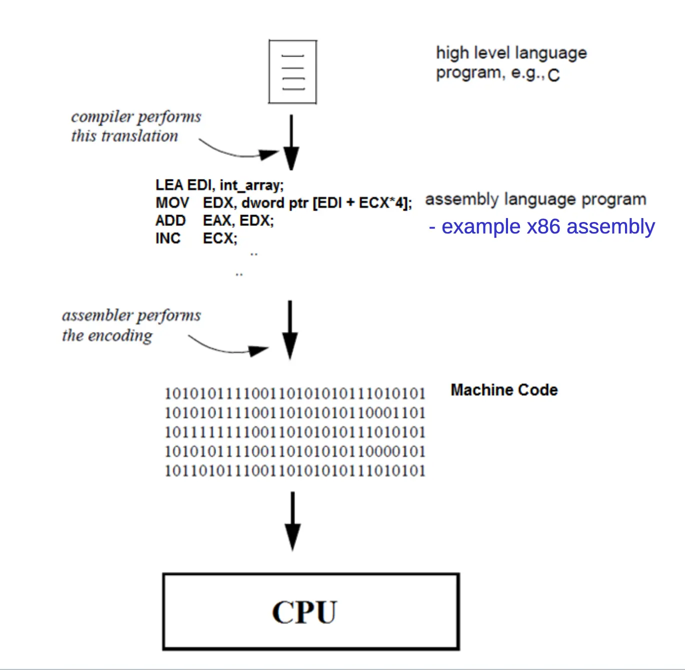
- How to execute a high-level language (L1) on standard hardware?
- Translate it to machine language (L0)
- Replace the entire program with its machine language equivalent
- Interpret it
- Take one instruction in the high-level language and execute it on the spot
- Translate it to machine language (L0)
- This process is done by compilers and interpreters
- The end result is the same
- Can think of this as a “virtual” machine M1 for L1
- It executes L1 as far as the user is concerned
- Does not matter if compiled or interpreted
- The “computer” is the interpreter + hardware together
- M1 hides the details of M0 → provides a new abstraction
Aside: Interpreters vs Compilers
- Interpreters take code and execute the equivalent low-level instructions on the fly
- Must re-interpret every time the program runs
- Checks what type of statement it is every time → overhead adds up
- Compilers translate the entire program once into lower-level code (e.g., assembly)
- More efficient at runtime
- Translate once, then every execution afterward runs native assembly/machine code
The M/L Hierarchy (Levels of Abstraction)
┌─────────────────────────────────────────────────────┐
│  Level 5 (M5 / L5)  │  High-Level Language (C, Java)│
├─────────────────────────────────────────────────────┤
│  Level 4 (M4 / L4)  │  Assembly Language            │
├─────────────────────────────────────────────────────┤
│  Level 3 (M3 / L3)  │  Operating System Machine     │
├─────────────────────────────────────────────────────┤
│  Level 2 (M2 / L2)  │  Instruction Set Architecture │
│                     │  (ISA) — machine code (0s/1s) │
├─────────────────────────────────────────────────────┤
│  Level 1 (M1 / L1)  │  Microarchitecture level      │
│                     │  (microprograms, ALU control) │
├─────────────────────────────────────────────────────┤
│  Level 0 (M0 / L0)  │  Digital Logic (transistors,  │
│                     │  gates, flip-flops)           │
└─────────────────────────────────────────────────────┘
- Each level hides the complexity below it → same abstraction principle discussed in INF 43 (Wasserman 1996)
- Assembly (L4) looks much simpler than raw microcode (L1) because each assembly instruction gets translated down through the layers
- When people say “low-level language,” they usually mean L2 (ISA/machine code) or L4 (assembly) → anything below that is typically invisible to programmers and baked into the hardware
Hierarchy of Virtual Machines
- L1 and L0 must not be too different
- Otherwise translation or interpretation becomes impractical
- Example: try going from English directly to machine language
- But you can have a hierarchy of virtual machines
- Each machine/language pair defines a level
- Each new virtual machine
- Hides details of the level below
- Adds new, higher-level capabilities
- This is a structured way of looking at computers
Layered / Structured View
- Top-down from the highest, most abstract layer
- A layer
- Groups together similar elements
- Abstracts away details of what’s below → they are not visible through this layer’s abstraction
- This way of looking at a computer system
- Simplifies understanding of the system
- Hides complexity
- At the bottom (for us) is hardware → transistors, etc.
- In reality there are layers below that
- (Fortunately for us) → EEs, physicists, chemists, and material scientists deal with them
- Hardware drives the definition of many basic issues
Example of Hardware Influence
- Digital hardware has 2 states (on/off)
- Memory speed depends on its type and size → computers use a hierarchy of memories
- A few registers (typically 32) → short-term storage
- Main memory (512KB - 128MB) → intermediate storage
- Disk (typically 100+ GB) → permanent storage
- Where is a variable declared in your C program located?
- Different places at different times → depends on the compiler
- These details are hidden from the programmer by the intervening layers
Layer Breakdown: Top to Bottom
Application Program Layer (L5)
- Written in a high-level language to solve a problem
- A very abstract view of the computer
- Named variables, if/case statements, loops, and functions
- Not directly understandable by standard hardware
- Requires translation to run on a computer system
- Large mismatch between hardware and these high-level abstractions
- Compilation into lower-level language (typically assembly or machine language)
- Which is still not directly executed by hardware
- Exception: Java is translated to bytecodes and interpreted
- Uses function libraries supplied by compilers and the OS (printf(), log(), etc.)
Assembly Language Layer (L4)
- Lower level of abstraction → more of the hardware directly exposed
- Registers and memory are used explicitly
- Operators (instructions) are much simpler
- Cannot say
A[I] := A[I] * B[I-3]anymore → need tedious details - Ends up using machine instructions like
ADD Rx, Ry
- Cannot say
- Still higher than machine language (binary)
- Views a computer as an Instruction Set Architecture
- Has access to OS-level abstractions
Operating System Layer (L3)
- Implements multiprogramming
- Ability to run multiple programs “simultaneously”
- Time-sharing the computer’s resources
- Allows a privileged mode of execution
- Direct access to certain hardware resources
- Protection
- System from user
- User from others and themselves
- Provides several major abstractions to a programmer
- File systems
- Virtual memory
- Process creation and scheduling (including loading a program and initiating its execution)
- I/O devices
- Networking
- Access to OS functions is through the system call interface
Instruction Set Architecture Layer (L2)
- ISA is the assembly programmer’s view of a computer
- Provides the following abstractions
- Data types → 8, 16, 32-bit integers, ASCII characters, etc.
- Operations (instructions) →
ADD Rx, Ry, Rzwhich implements Rx ← Ry + Rz - Addressing modes
- Memory model and addressing → word size, byte order, number of words
- Registers
Microarchitecture Layer (L1)
- Also called computer organization → describes
- Major units of a system → ALU, register file, control unit, memory, caches, I/O
- How they are interconnected → e.g., ALU is only connected to registers
- Protocols for their communication
- Synchronous (clock-based)
- Asynchronous (handshake-based)
- Abstracts away the digital logic and hardware layers
- They contain the same information but at a much more detailed level, plus additional info like voltage levels and timing
Digital Logic Layer (L0)
- Describes a computer at a gate level
- Gates are the basic building blocks → AND, OR, NOT, 1-bit storage element
- Shows gate-level implementation → an adder is described as a number of logic gates and their connections
- Some hardware details are still abstracted away
- Timing information is much simpler
- Analog nature of transistors can be ignored → treat them as digital switches (ON or OFF)
Hardware Layer (Below L0)
- Describes a computer at the transistor level
- Every transistor and its connection to others
- There are >10 BILLION transistors in a modern state-of-the-art processor
Why Use Abstraction?
- 10 billion transistors in a processor alone, plus much more in memory, I/O devices, and controllers
- Impossible to design without abstractions → so the work is divided → SE faces the same complexity problem
- One group designs the semiconductor process
- Another group designs several different transistors → needs only some key parameters from the process
- Another group designs dozens of gates and memory cells → doesn’t need process info, just transistor parameters
- Computer engineers use gates to design a processor → only deal with gates, memory cells, and their parameters
Lecture 2: System Organization
System Overview
┌─────────────────┐
│       CPU        │
│ ┌─────────────┐  │
│ │ Control Unit│  │
│ └─────────────┘  │
│ ┌─────────────┐  │
│ │     ALU     │  │
│ └─────────────┘  │
│ ┌─────────────┐  │
│ │  Registers  │  │
│ │ ┌──┬──┬──┐  │  │
│ │ │  │  │  │  │  │
│ │ ├──┼──┼──┤  │  │
│ │ │  │  │  │  │  │
│ │ └──┴──┴──┘  │  │
│ └─────────────┘  │
└────────┬─────────┘
         │
═════════╪══════════╪══════════╪══════════╪═══  BUS
         │          │          │          │
    ┌────┴────┐ ┌───┴───┐ ┌───┴───┐ ┌───┴────┐
    │ Memory  │ │ Disk  │ │Printer│ │  ...   │
    └─────────┘ └───────┘ └───────┘ └────────┘
- CPU → Central Processing Unit (same as processor)
- Consists of data path and control unit
- Data path = ALU + register file
- Control Unit → directs operations
- ALU → performs arithmetic and logic
- Registers → small, fast storage (grid of cells)
- Memory → DRAM + controller, always byte-addressable
- Bus → a collection of wires for communication between all components
- Master sends commands/data, slaves respond with data or write
- Manager/Worker (Master/Slave) protocol → dictates who has access to the bus
- Wires are the most important part → expensive, and the bottleneck of the computer
I/O Devices
- Devices are viewed as memory (disk, printer, screen)
- Why? → They are simple receivers and senders of binary data
- Read/write data from/to them
- Each usually has a controller that understands its operation → special-purpose processor
- CPU is freed to do other things while the controller handles the device
A Simple Data Path
                       Reg_addr A ----┐
                       Reg_addr B ----┐
  Result addr ---┐                    │
                 ▼                    ▼
          ┌──────────────────────┐
          │    Register File     │
          └───────┬────────┬─────┘
                  │ A      │ B
                  ▼        ▼
   Cin ------→┌──────────────┐
  ALU_op ----→│     ALU      │──→ [Z]
              └──────┬───────┘──→ [N]
                     │         ──→ [C]
                     ▼
                   Result
                     │
                     └──────────→ (back to Register File)
- Register File
- Inputs (control, dashed): Result addr, Reg_addr A, Reg_addr B
- Input (data, solid): Result writeback from ALU output
- Outputs (data): A and B → fed into ALU
- ALU
- Data inputs: A (left operand), B (right operand)
- Control inputs (dashed): Cin (carry in), ALU_op (operation select)
- Data output: Result → feeds back to register file
- Flag outputs: Z (zero), N (negative), C (carry)
- This is a high-level description of the data path → there are circuits underneath that dictate the compute logic
- ALU takes operands from the register file and writes the result back to a register
- Thick lines → buses, dotted lines → control wires (controlling what we do, not directly part of the computation)
Data Path Operation
- Read operands from the register file (A and B)
- At current rising edge of the clock signal
- Most machines run off a clock that gives precise timing for when each cycle starts
- In principle, asynchronous (non-clocked) designs are not actually faster compared to clocked machines
- Place on buses A and B
- At current rising edge of the clock signal
- Specify ALU operation → add, multiply, etc.
- “Wait for ALU”
- Designed to fit into 1 clock cycle → no real wait, damn near instant (nanoseconds) → this is the “+1 operation” cost in T(N) analysis
- Machine is designed around the longest operation
- Sometimes an operation finishes early but we wait for the clock anyway
- Write result from bus C to selected register → on the next rising edge
- Set flags: N, C, Z
- These are single-bit registers
- Whatever operation came through the ALU (multiply, add, etc.) sets specific flags based on the output
- These are the fundamental building blocks that allow conditional operations
- This is what x86 does when executing
ADD R4, R6or similar RR (register-to-register) operations
Memory View
- Linear array of words → each word 2 or 4 bytes
- Memory is byte-addressable, even if typically organized as “words”
┌─────────┬─────────┐
│ Byte 0  │ Byte 1  │  Word 0
├─────────┼─────────┤
│ Byte 2  │ Byte 3  │  Word 1
├─────────┼─────────┤
│         :         │
│         :         │
├─────────┴─────────┤
│                   │  Word N-1
└───────────────────┘

Each row is one word (2 bytes wide)
Word addresses: 0, 1, ..., N-1
Total: N words, 2N bytes
Other Data Path Organizations (Operand Specifiers)
- x86 (32-bit) and our example use 2-address instructions (2 operand specifiers per instruction)
- Can be changed to:
- 3-address → source and destination registers can be distinct
R[4] ← R[8] + R[6]- More bits needed in each instruction
- 1-address → one source operand and the destination are predefined
- Uses a special register called the accumulator
- Operations are of the form
ACC ← ACC + R[6] - Price: irregularity → requires an extra step to load/store the accumulator
- 0-address → both source operands and the destination are predefined
- Stack machine → special register points to the top of the stack
- All operands must be pushed/popped on the stack
- Operations are of the form
stack[top] ← stack[top] + stack[top+1] - Example: old HP calculators (Reverse Polish Notation)
- Useful for evaluating deeply nested expressions
- 3-address → source and destination registers can be distinct
Register Transfer Language (RTL)
- A shorthand for describing data path operations
R[4] ← R[4] + R[6]Z ← 1 if R[4] = 0
- Can describe simultaneous (parallel) operations
MDR ← Mem[MAR] ; PC ← PC + 2
- Useful shorthand for describing register-to-register operations
- Same notation can be used for control logic
CPU Instruction Execution Cycle
- CPU executes an instruction in several steps
- Do forever:
- Fetch instruction from memory into Instruction Register (IR)
- Increment Program Counter (PC)
- Decode the instruction in IR
- Fetch operands specified by a field in IR
- Execute operation specified by a field in IR
- Store result (if necessary) as specified by a field in IR
- This cycle repeats forever until a halt instruction stops the processor
- This is the algorithm for the control unit
Execution Cycle in RTL
- Instruction Fetch →
IR ← Mem[PC] - Increment Program Counter →
PC ← PC + 2 - Decode → generate all necessary control signals
- Fetch Operands →
A ← RegFile[IR(src1)],B ← RegFile[IR(src2)] - Execute Operation →
Result ← ALU(IR(opcode), A, B) - Store Result →
RegFile[IR(dest)] ← Result
Instruction Set Architecture (ISA)
- Consists of
- Memory model
- Data types
- Addressing modes → how instructions specify RAM locations
- Instructions
- Instruction format
ISA Details (Assuming Intel x86)
- Memory model
- 4GB of memory
- Byte-addressable
- Linear array of storage locations
- 8-byte physical word
- Registers
- Eight 32-bit integer registers, some “reserved” for specific tasks (e.g., Stack Pointer)
- Can be used as 16-bit or 32-bit using different mnemonics
- Plus special registers → program counter, flags, etc.
- Some not directly accessible to the programmer (cannot add to program counter directly)
- Data types
- Integer, floating point, decimal, ASCII
- Operations defined on each type
Addressing Modes
- How instructions specify memory locations
- Using registers, immediate operands, memory addresses
- How many operands → 0-, 1-, 2-, and 3-address instructions
- Instruction format
- Specifies size and “fields” in the instruction word
- Typical fields: opcode, source operand specifiers, result specifier
Instruction Design
- Instructions can be grouped by type
- Arithmetic → +, -, *, /
- Logical → AND, OR, NOT, XOR, shifts
- Control → conditional branches, jumps (change PC)
- Move → memory to register, register to register
- x86 instructions have many formats and addressing modes → too many to cover
- Also has real, virtual, and protected modes → for backwards compatibility, security, etc.
Example x86 Instructions
MOV R1, 4
- Type: move
- Destination: R1 (register 1)
- Addressing mode: immediate
- The constant 4 requires at least a 4-bit data type
MOV AX, [02D]
- Type: move
- Destination: AX (16-bit register; EAX is 32 bits)
- Addressing mode: direct addressing
- Address is really
DS:[02D]
JMP label1
- Type: jump
- Destination: label1
- Transfers control to the instruction located at label1
Lecture 3: Data Representation & Digital Logic
Data Representation
- Computers represent everything in binary
- This includes programs, input/output information, and intermediate variables
- ASCII table provides mapping of 8 bits (1 byte) to characters
0100 0001in binary → character “A” in ASCII
- Binary, octal, or hexadecimal for integers
- Floating point for real numbers
Binary Numbers
- Base 2 number system compared to our regular base 10
- Digits: 0 and 1
- Positional system → 101 decimal = 100 + 1
- A binary number
111means:- 1 × 2² + 1 × 2¹ + 1 × 2⁰ = 7 (decimal)
Octal
- Base 8 system
- Digits: 0–7
555omeans:- 5 × 8² + 5 × 8¹ + 5 × 8⁰ = 365 (decimal)
- Bytes (8 bits) are typically written in octal for convenience
Hexadecimal
- Base 16 number system
- Digits: 0–9, A (10), B (11), C (12), D (13), E (14), F (15)
ABCh= 2748d- 10 × 16² + 11 × 16¹ + 12 × 16⁰ = 2748
- Bytes (8 bits) are sometimes also written in hex for convenience
Digital Hardware Level
- Computers are built using gates and memory
- Simplest building blocks at this level of abstraction → digital logic / computer organization level
- Gates and memory are made with transistors
- Can be viewed as electronic switches in digital logic
- They connect or disconnect based on the input value → gives rise to two-value (binary) system
- Another abstraction — reality is much more complex
- Transistors are the building blocks at the hardware level
- Can be viewed as electronic switches in digital logic
- Information values are voltage values
- +3.3V → “One”, 0V (ground) → “Zero”
- aka “high” and “low” (T/F) values or states
- +3.3V → “One”, 0V (ground) → “Zero”
- Digital circuits can only be in one of these two states
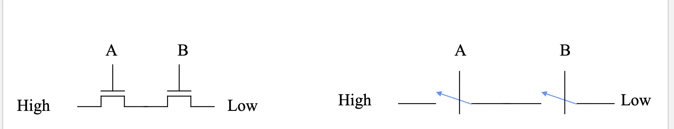
CMOS Transistors
- Don’t have to know much about this — all it does is open and close
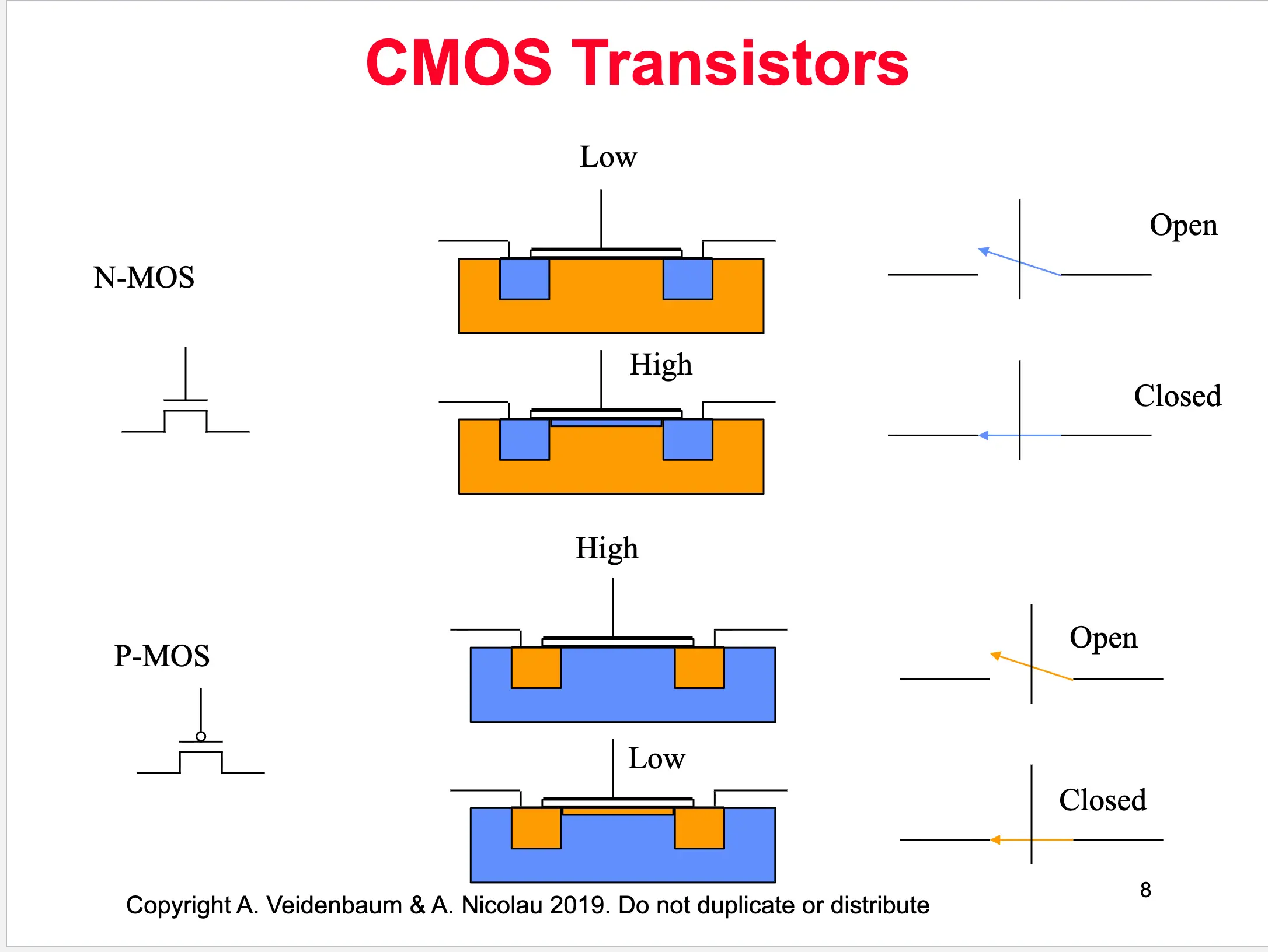
- Gates implement basic boolean functions such as AND, OR, NOT
- Implemented using two voltage “rails” → High and Low
- The output connects to one rail at a time, giving it a desired value
- Input values A, B determine which rail
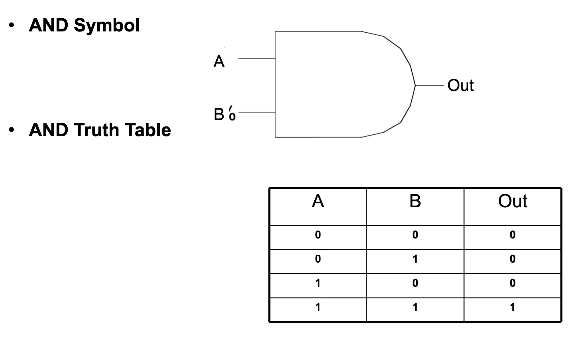
- Consider an AND gate:
- AND function → SERIES connection to High value
- OR function → PARALLEL connection to High
- Must always be connected to one or the other (high/low), otherwise electronics fails
CMOS AND Gate
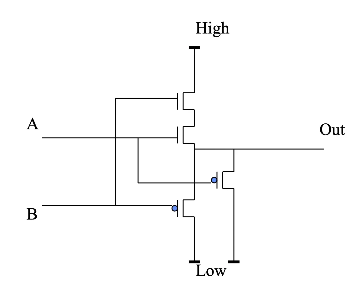
- Out connects to High only when BOTH A and B are High (N-MOS transistors)
- Out connects to Low when either A or B (or both) are Low (P-MOS)
Truth Table Walkthrough
- We just made a digital gate — what is its function?
- A=Low, B=Low → Out=Low
- A=High, B=Low → Out=Low
- A=Low, B=High → Out=Low
- A=High, B=High → Out=High
Logic Gates
- A gate has one or more inputs and one output
- Standard symbols represent common gates
- Logically, a gate represents a Boolean function on input variables
- All variables are Boolean (binary) values
- A truth table lists all possible combinations of values of the input variables
Boolean Algebra
- Behavior of gates can be described with Boolean Algebra
- Abstracts away hardware characteristics
- An algebra → a set of values and operations with certain properties
- Similar to a data type in a programming language
- Boolean Algebra:
- {0, 1}, OR, NOT
- Values are 0, 1; operations are OR and NOT
- A computer can be built using just these two
- Values are 0, 1; operations are OR and NOT
- Typically use additional operators: AND, etc.
- {0, 1}, OR, NOT
Boolean Operators
- NOT (negation, complement, inverse)
- Y = NOT(X) = X’
- OR (union, disjunction, logical sum)
- Y = X + Z = X OR Z
- AND (conjunction, logical multiplication)
- Y = X · Z = X AND Z
Logic Gate (AND) with Truth Table
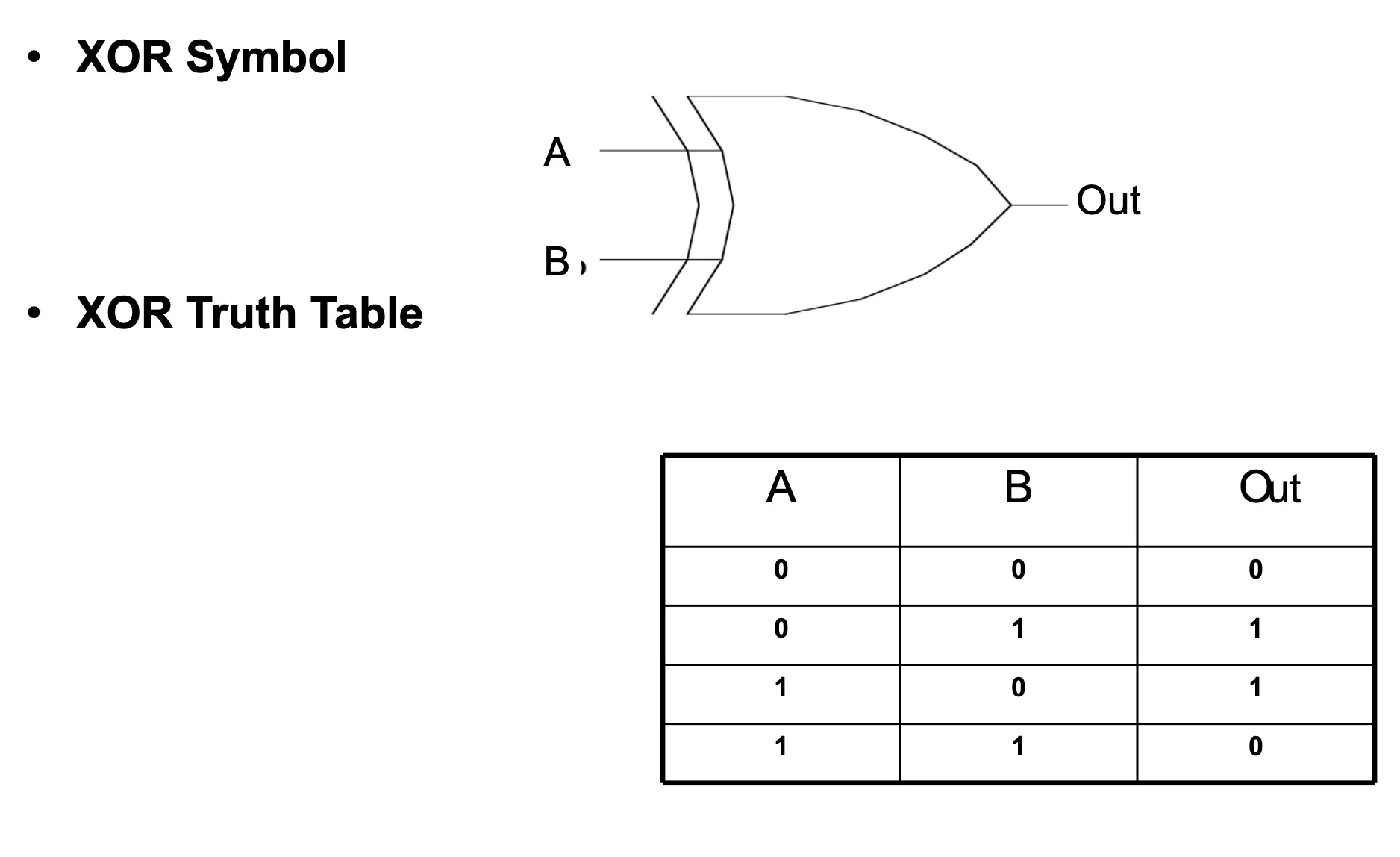
Logic Gate (XOR) — Exclusive OR with Truth Table
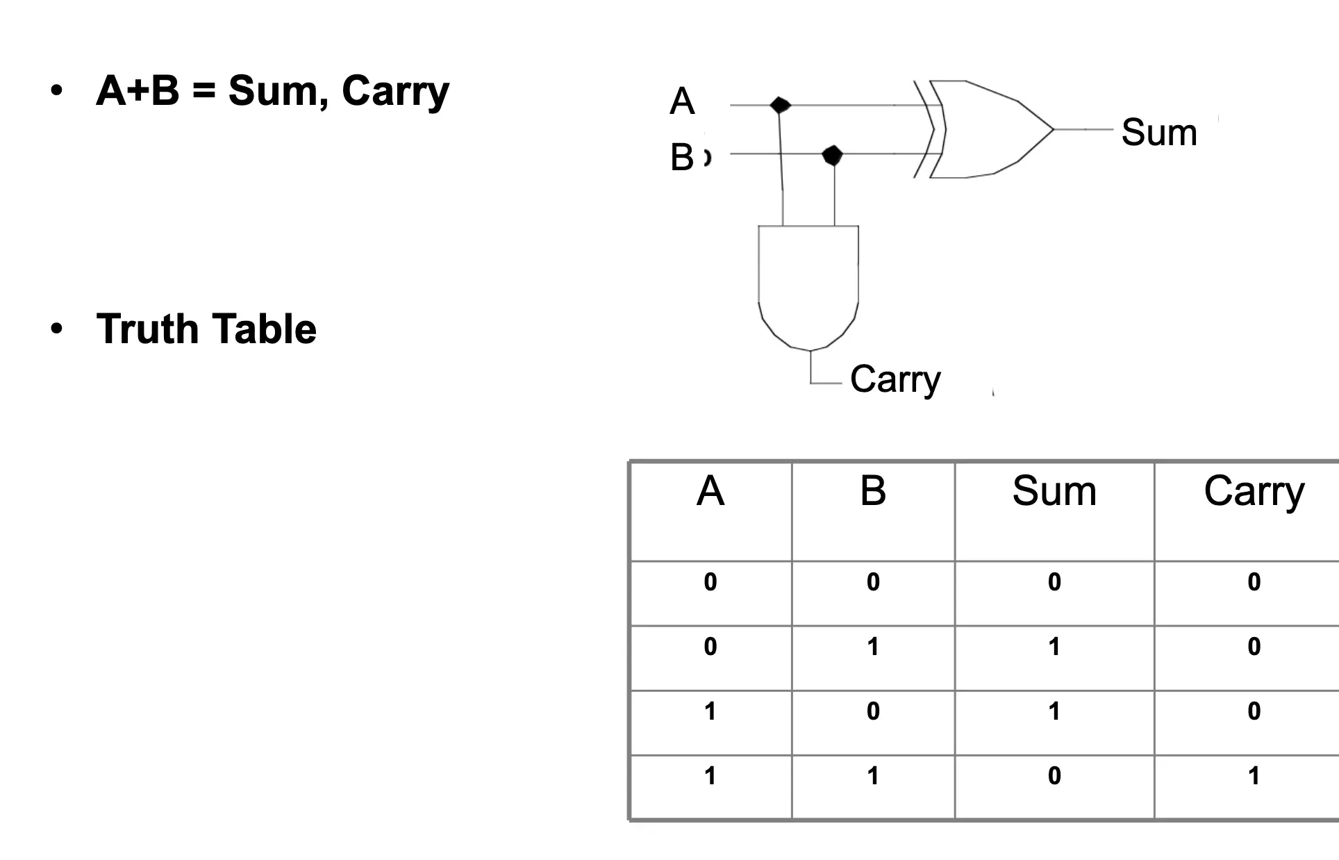
One-Bit Adder
Boolean Functions
- Used to describe most of the data path elements
- Out = F(IN₀, IN₁, …, INₙ₋₁)
- n-input functions with 1 output
- Both inputs and output are 1-bit binary variables
- Out = F(IN₀, IN₁, …, INₙ₋₁)
- Composable from NOT, AND, OR, etc.
- Each of those is itself a Boolean function
- Even just OR + NOT (NOR) is sufficient for everything
- Or AND + NOT (NAND)
- Boolean Algebra provides:
- Mathematical foundation
- Theorems for transforming functions → obtaining a different but equivalent function
- Equivalent → same inputs produce same output value
Symbols and Terminology
- AND → often shown as · (multiply), A · B
- Or even simply AB
- These are called product terms (Π)
- OR → often shown as + (sum), A + B
- Or even Σ
- ΣΠ → a sum of products
- Or even Σ
- NOT → shown with a bar or accent over a symbol
- NOT(A) = Ā = A’
Boolean Operator Precedence
-
NOT → highest
-
AND
-
OR → lowest
-
Thus:
- NOT A AND B = (NOT A) AND B
- A OR B AND C = A OR (B AND C)
Function Description
- A function can be described by a truth table
- Unlike functions in “normal” algebra
- Because Boolean algebra has a small set of inputs
- 4-input function → 2⁴ possible input combinations → can just enumerate them
- From truth table → obtain a canonical form
- A sum of product terms which make output = 1
- Each term shown with either true or complement of inputs
- A’BC’ → means Out = 1 when A = 0, B = 1, C = 0
- Sum is a big OR gate
- Each term shown with either true or complement of inputs
- A sum of product terms which make output = 1
Example: XOR Gate
- Product terms that make output = 1:
- A’ · B → AND of (NOT A) and B
- A · B’ → AND of A and (NOT B)
- Sum of products:
- Out = A’ · B + A · B’
Design Algorithm for Boolean Functions
- Write a specification for a Boolean function → what needs to be implemented
- Fill in the truth table
- Write the sum of product form
- Only for each term that has a
1in the output column
- Only for each term that has a
- Draw the logic gates needed:
- Draw inverters for inputs that need a complement
- Draw an AND gate for each product term used
- Connect (wire) inputs to the AND gates
- Draw an OR gate for the sum
- Wire outputs of AND gates to the OR gate
Discussion 1: Introduction to MIPS Assembly
- High-Level Language → (compiler) → Assembly → (assembler) → Machine Code → CPU
A Typical Computer Architecture
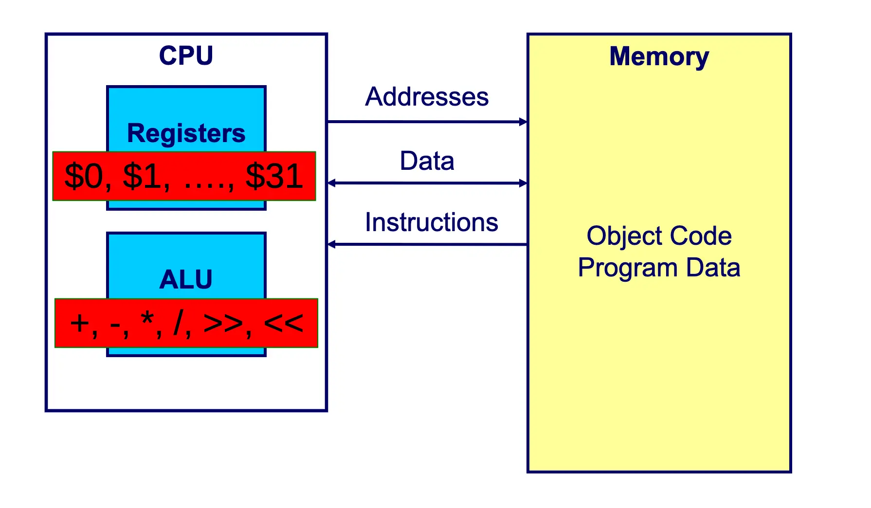
- CPU
- Registers → 1, …, $31
- ALU → +, -, ·, /, <<, >>
- Between the two, addresses come into memory; data and instructions come out of memory
- Memory → object code, program data
Registers
- CPU needs internal fast storage to store intermediate computation results and frequently used data
- Registers are faster than memory
- MIPS has 32 general-purpose registers, each 32 bits wide
- Called a 32-bit architecture
- MIPS registers can be identified by their index → 0, 31)
MIPS Register Set
| Name | Register # | Usage |
|---|---|---|
| $0 | 0 | The constant value 0 |
| $at | 1 | Assembler temporary (reserved) |
| v1 | 2-3 | Function return values |
| a3 | 4-7 | Function arguments |
| t7 | 8-15 | Temporaries (not preserved across function calls) |
| s7 | 16-23 | Saved variables (preserved across calls) |
| t9 | 24-25 | More temporaries |
| k1 | 26-27 | OS temporaries (reserved for OS) |
| $gp | 28 | Global pointer |
| $sp | 29 | Stack pointer |
| $fp | 30 | Frame pointer |
| $ra | 31 | Function return address |
Operands: Registers
- Registers used for specific purposes (Register Convention):
- a3 → used to pass arguments into subprogram
- v1 → used for return values for subprogram OR system services (syscall)
- t9 → used to hold intermediate values; values can change when a subprogram is called
- s7 → used to hold variables; values are maintained across subprogram calls
- Special registers other than 31:
- pc, lo, hi
Memory
- From the programmer’s point of view, memory is a contiguous array of bytes (8-bit data values)
- The index of each element in the array is called an “address”
- For a 32-bit processor, the address range is from 0 to 2³² − 1
- 2³² bytes = 4 GB
- In MIPS, it is only possible to read/write from/to memory 1/2/4 bytes in a single operation
- 1 word = 4 bytes
- 1 half word = 2 bytes
Instructions with Registers (ADD)
- C code:
a = b + c - MIPS Assembly:
# $t0 = a, $t1 = b, $t2 = c
add $t0, $t1, $t2
MIPS Instructions
- MIPS instructions have the following format:
[label:] operation [operands] [#comment]
iamalabel:
add $t1, $t2, $t3 # this is a comment- Labels are optional → instead of counting lines, you give a location a name
- Operations → add, sub, addi, sll, beq, etc.
- Operands specify the data required by the operation
- Can be register names, constant numbers, or memory locations/addresses (where you put labels)
- The instruction format depends on the operation
MIPS Program Template (.asm vs .c)
###### Data segment ######
.data
# define program data such as arrays here
array_a: .space 40

###### Code segment ######
.text
# define other functions if any
foo:
    # foo function entry … logic …
main:
    # main program entry
    # … program logic, calling other functions…
    li $v0, 10       # Exit program
    syscall          # using a system call
/****** Data segment ******/
int array_a[10];
/****** Code segment ******/
int foo(){…}
int main(){
// main program entry
// … program logic, calling other functions…
return 0; // Exit program
}- Data Directive
- Defines the data segment of a program containing data
- The program’s variables should be defined under this directive
- Text Directive
- Defines the code segment of a program containing functions and assembly instructions
- To define main as the entry point of the program:
- In MARS, toggle Settings → Initialize Program Counter to global main if defined
- Place
.globl mainunder.text
- To define main as the entry point of the program:
- Defines the code segment of a program containing functions and assembly instructions
Instruction Types
- Arithmetic instructions
- Logical instructions
- Data movement instructions
- Register ↔ register
- Memory ↔ register (load/store)
- System calls
- Comparison instructions
- Control transfer instructions
- Unconditional (jump)
- Plus stack pointer (i.e. for function calls)
- Conditional (branch)
- Unconditional (jump)
Arithmetic Instructions
add $dst, $src1, $src2     # $dst = $src1 + $src2
sub $dst, $src1, $src2     # $dst = $src1 - $src2

mult $src1, $src2          # {hi, lo} = $src1 * $src2
div $src1, $src2           # lo = $src1 / $src2
# hi = $src1 % $src2- Examples:
add $t3, $t1, $t2          # $t3 = $t1 + $t2
sub $t3, $t1, $t2          # $t3 = $t1 - $t2
mult $t1, $t2              # {hi, lo} = $t1 * $t2
Arithmetic Instructions (Immediate)
addi $dst, $src1, $imm # $dst = $src1 + $imm
addi $t3, $t1, 5 # $t3 = $t1 + 5
addi $t3, $t1, -20 # $t3 = $t1 + (-20)
addi $t3, $t1, $t2 # WRONG! (can't use register as immediate)
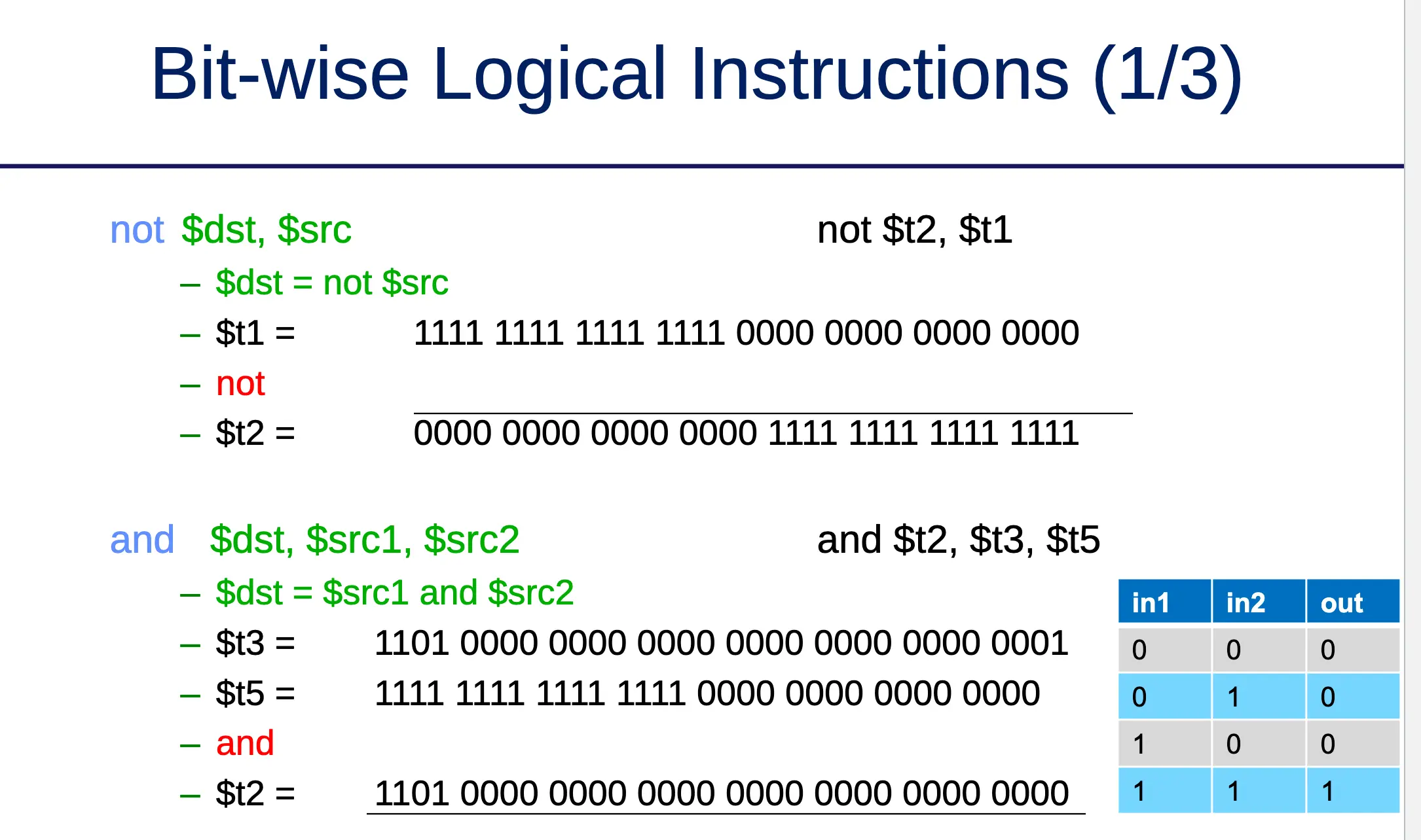
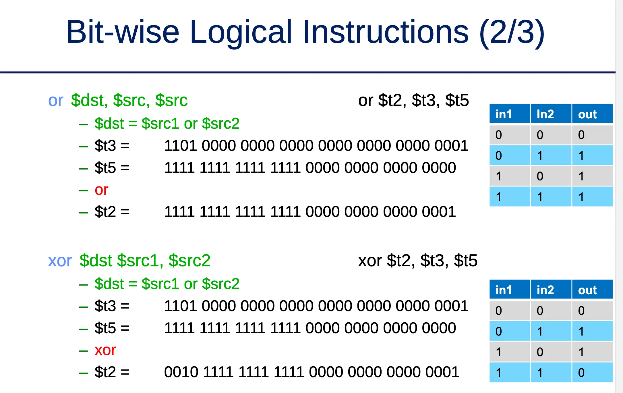
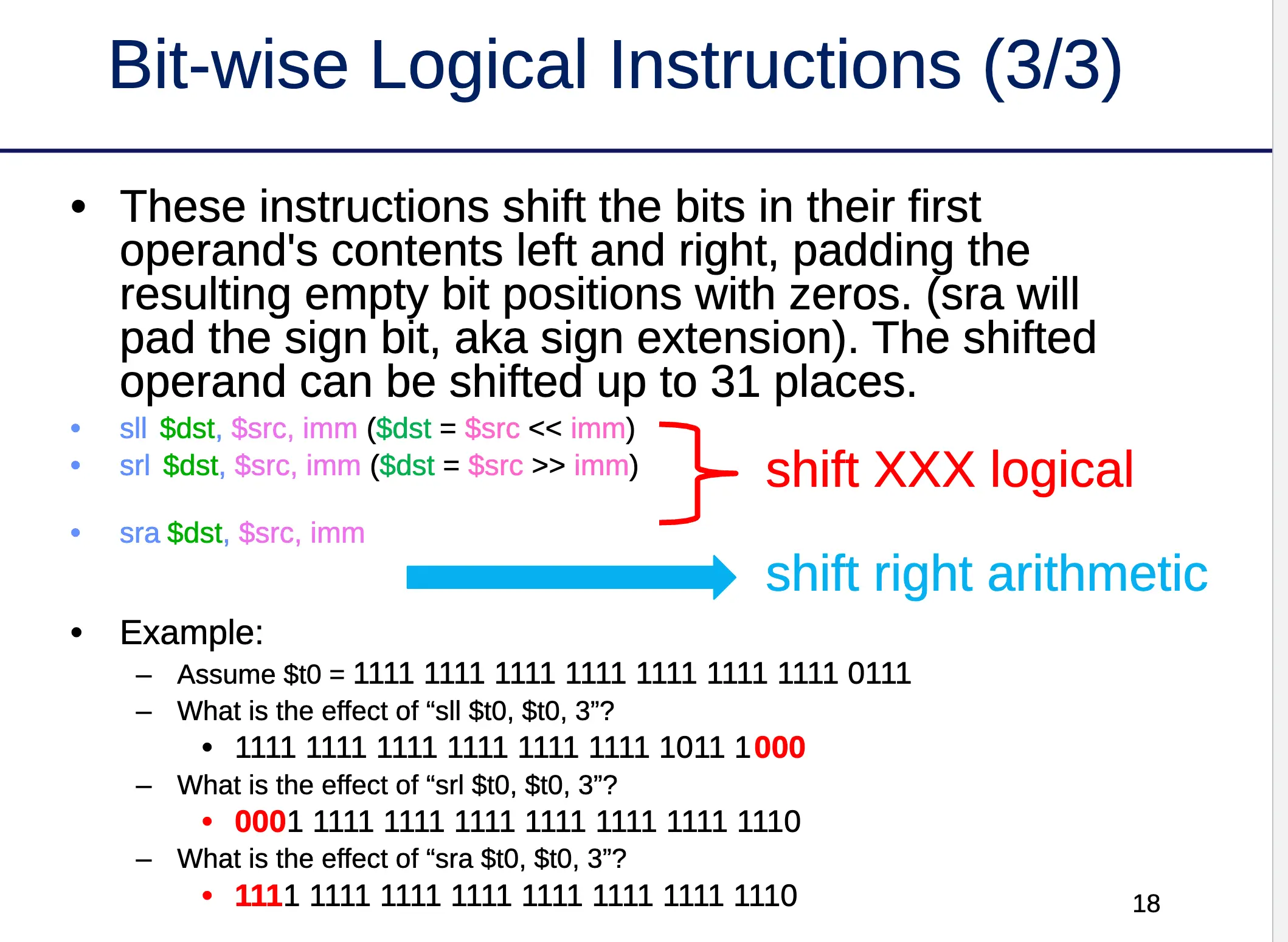
add $t3, $t1, $t2 # CORRECT!Bit-Wise Logical Instructions
Data Movement Instructions
- Move (copy) value between registers:
add $dst, $src, $zero→ e.g.add $t1, $t0, $zeromove $dst, $src→ e.g.move $t1, $t0
- Load value → from a memory address into a register
- Store value → from a register into a memory destination
MIPS Pseudo-Instructions
- Pseudo-instructions are provided by the assembler but do NOT have the operation implemented in hardware
- They get translated into multiple simple instructions
- Example:
move $t0, $t1- Translates into →
addu $t0, $t1, 0 - Other possible translations:
add $t0, $t1, $0or $t0, $t1, $0
- Translates into →
Example of MIPS Pseudo-Instruction
mult(basic instruction)mult $t0, $t1→ hi, lo = t1
mul(pseudo-instruction)mul $dst, $src1, $src2- Translates into:
mult $src1, $src2mflo $dst
System Calls
- MIPS provides a special
syscallinstruction to obtain services from the operating system- Many services are provided in the MIPS simulators → reading/writing files, console
- To use syscall system services:
- Load the service number in register $v0
- Based on the spec, load argument values into register $aX
- Launch the
syscallinstruction - Retrieve return values, if any, from result registers
- Example → end program:
li $v0, 10
syscall
MIPS Instruction Set References
- Press F1 → Help menu in MARS
- MIPS instructions → https://www.dsi.unive.it/~gasparetto/materials/MIPS_Instruction_Set.pdf
- MIPS pseudo-instructions → https://github.com/MIPT-ILab/mipt-mips/wiki/MIPS-pseudo-instructions
- MIPS syscall functions → http://courses.missouristate.edu/kenvollmar/mars/help/syscallhelp.html
MIPS Emulator
- Hard to find a MIPS processor in the wild → we use programs that emulate MIPS machines
- MARS (also used for grading labs) → https://courses.missouristate.edu/KenVollmar/mars/download.htm
- SPIM and QtSPIM → available for Linux, macOS, and Windows → https://sourceforge.net/projects/spimsimulator/files/
Discussion 2: Bit Masking, Multiply by Shift-and-Add, Conditional Statements
Bit Masking
- Use bitwise logical instructions to:
- Set bit values to 1
- Clear bit values to 0
- Query bit values
- Mask → a special binary number used together with logical instructions to set, clear, or query specific bits
Setting Bits (OR)
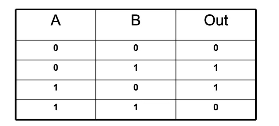
- OR truth table
- OR with 0 → no change
- OR with 1 → result is 1
Clearing Bits (AND)
- AND truth table
- AND with 0 → result is 0
- AND with 1 → no change
Querying Bits (AND)
- Use bitwise AND to query specific bits
- Clear all bits except the ones you want to query
- Example: query the value of bit 3
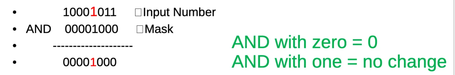
- In assembly (assume
$t0has the input number)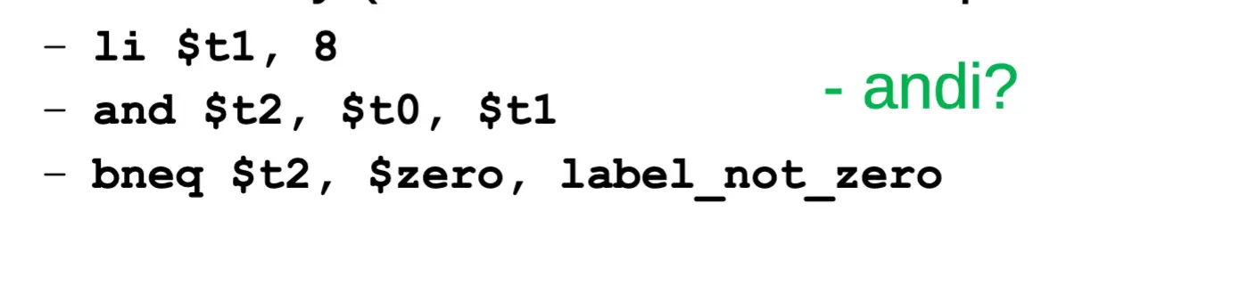
Example: Clearing/Querying Multiple Bits
- Example → query odd bits of an integer (= clear even bits of an integer)
- Use AND operation
- AND with 0 → 0
- AND with 1 → no change
- Mask will be 32 bits wide
- Use
1010_1010_1010_1010_1010_1010_1010_1010as mask- 0 for bits we want to clear
- 1 for bits that need to keep their value
0xAAAAAAAAin hex OR2863311530in decimal- You can’t write binary literals in MIPS assembly
- Use AND operation
- In assembly:
li $t1, 0xaaaaaaaa
and $t0, $t0, $t1
Multiplication & Division (MIPS)
- Special registers →
lo,hi - 32 × 32 multiplication, 64-bit result
mult $t0, $t1→ result in {hi,lo}
- 32-bit division → 32-bit quotient, 32-bit remainder
div $t0, $t1→ quotient inlo, remainder inhi
- Moves from
lo/hispecial registersmflo $t2mfhi $t3
- Or use
mul $t2, $t0, $t1(pseudo-instruction)
Sequential Binary Multiplication
         1 0 1 1   (multiplicand = 11)
       × 1 1 1 0   (multiplier   = 14)
       ==========
         0 0 0 0
       1 0 1 1
     1 0 1 1
 + 1 0 1 1
 ==================
   1 0 0 1 1 0 1 0  (product = 154)
Multiply by Shift-and-Add
- Binary number 0000_0001_0010 → position values are 2ⁱ (128, 64, 32, 16, 8, 4, 2, 1)
- Digit × position value → 0 + 0 + 0 + 16 + 0 + 0 + 2 + 0 = 18
- If we shift the number 1 bit to the left (
<< 1) → 0000_0010_0100- Now: 0 + 0 + 32 + 0 + 0 + 4 + 0 + 0 = 36
- Shifting one bit left doubles the number (18 → 36)
- Key insight:
- Shifting an integer by n bits to the left = multiplying by 2ⁿ
- Shifting an integer by n bits to the right = dividing by 2ⁿ
- How to multiply
$t2by 2 using shift in assembly →sll $t2, $t2, 1 - Multiply by 16 → 16 = 2⁴ →
sll $t2, $t2, 4 - Multiply by 18 → 18 = 16 + 2 → shift-and-add both
General Case: Multiply N by M (non-power of two)
- Decompose M into sum of powers of two (use binary representation)
- Multiply N by each component using shift
- Add all partial results together
- Example: 13 · N
- 13 = 8 + 4 + 1 (binary: 0000_1101)
- 13·N = (8 + 4 + 1)·N = (N<<3) + (N<<2) + N
Assembly Control Flow
- Assembly instructions execute sequentially
- Program Counter (
$pc) → special register pointing to the next instruction to execute - Default behavior: PC ← PC + 4
- Memory layout example:
Address        Instruction
0x0040_0000    addi $t0, $t1, 1
0x0040_0004    and  $t2, $t1, $t0
0x0040_0008    move $t3, $t2
...
Changing the Execution Flow
- Use jump instructions to skip a block of code
- Equivalent to changing
$pcto something other than PC + 4 - Example: jump from
addi $t0, $t1, 1directly tomove $t3, $t2, skipping theandin between - Need to know either:
- The destination address, OR
- The relative offset
- Two flavors: unconditional jump or conditional branch
Unconditional Jumps
j label→ jumps to first instruction after the label- PC ← coded 26-bit address of label
jal label→ jump and link- Link → next instruction address after
jalis loaded into$ra - Used for function calls (future discussion)
- Link → next instruction address after
jr $reg→ jumps to address in$reg- PC ←
$reg - e.g.
jr $ra
- PC ←
Conditional Branches
- Compare on:
- Equality/inequality of two registers
beq $t0, $t1, target→ branch to target if$t0 == $t1
>,<,>=,<=of a register and 0bgtz $t0, target→ branch if$t0 > 0
- Equality/inequality of two registers
| Condition | Instruction |
|---|---|
| equality | beq |
| inequality | bne |
| > 0 | bgtz |
| < 0 | bltz |
| ≥ 0 | bgez |
| ≤ 0 | blez |
slt Instruction
slt $dst, $s, $t→ if$s < $t, set$dst = 1, else$dst = 0- Used to build pseudo-instructions for comparing two registers:
| Pseudo-instruction | Syntax | Expansion |
|---|---|---|
| branch if greater than | bgt $s, $t, C | slt $at, $t, $s / bne $at, $zero, C |
| branch if less than | blt $s, $t, C | slt $at, $s, $t / bne $at, $zero, C |
| branch if greater than or equal | bge $s, $t, C | slt $at, $s, $t / beq $at, $zero, C |
| branch if less than or equal | ble $s, $t, C | slt $at, $t, $s / beq $at, $zero, C |
If Statements
- Python:
if condition:
statements- Statements enclosed by
ifonly execute when the condition is true - Example:
if x > 5:
    z = 7
x = x + 1- Steps to execute:
- Evaluate the condition
x > 5 - If false → skip
z = 7and continue fromx = x + 1 - If true → execute
z = 7, then continue fromx = x + 1
- Evaluate the condition
Compiling If Statements
- Use a jump/branch to skip a block of code
- Template:
if condition:
    <<statements>>
translates to:
    test NEGATED condition
    if true → jump to EndOfIf
    <<statements>>
EndOfIf:
- Negated condition being true = original condition being false
- Example:
if (a < b) a++
move $t0, $a0
move $t1, $a1
bge $t0, $t1, EndOfIf   # bge is the complement of "<"
addi $t0, $t0, 1
EndOfIf:
If…Else Statement Translation
- Template:
if (condition):
    THEN block
else:
    ELSE block
translates to:
    test NEGATED condition
    bxx ElseCode
    <<THEN block>>
    j EndOfIf
ElseCode:
    <<ELSE block>>
EndOfIf:
- Example:
max = (a > b) ? a : b; max = max + 2
# $a0 = a, $a1 = b, $t2 = max
move $t0, $a0
move $t1, $a1
ble $t0, $t1, ElseCode
    move $t2, $a0
    j EndOfIf
ElseCode:
    move $t2, $t1
    # no need for j here → falls through
EndOfIf:
    addi $t2, $t2, 2
Complex If Statements: AND (&&)
if (a == b && a > c) { <<stmts>> }is equivalent to nested ifs:
if (a == b) {
    if (a > c) { <<stmts>> }
}
- Assembly:
move $t0, $a0   # a
move $t1, $a1   # b
move $t2, $a2   # c

bne $t0, $t1, end_if
ble $t0, $t2, end_if
<<statements>>
end_if:
Complex If Statements: OR (||)
if (a == b || a > c) { <<stmts>> }is equivalent to:
if (a == b) {
    <<stmts>>
} else {
    if (a > c) { <<stmts>> }
}
- Assembly:
move $t0, $a0   # a
move $t1, $a1   # b
move $t2, $a2   # c

bne $t0, $t1, else_code
<<statements>>
j end_if
else_code:
    ble $t0, $t2, end_if
    <<statements>>
end_if:- Alternative method (branch into the if body):
beq $t0, $t1, if_code
bgt $t0, $t2, if_code
<<rest of program>>
# NOTE: add j to skip around if_code
if_code:
<<statements>>
# NOTE: add j instructions as needed to control flow
Sample Problem: Implement max
int max(int a, int b, int c)→ returns the maximum of three ints- C implementation:
int max(int a, int b, int c) {
    int max = a;
    if (b > max) max = b;
    if (c > max) max = c;
    return max;
}- Assembly (params in
$a0, $a1, $a2, return in$v0):
# int max = a
move $t0, $a0
# if (b > max) max = b
ble $a1, $t0, check_c
move $t0, $a1
check_c:
# if (c > max) max = c
ble $a2, $t0, ret_max
move $t0, $a2
ret_max:
move $v0, $t0
Lab1 / Register Convention Notes
- Do NOT use
$sX(saved) registers in Lab 1 unless you follow the register convention- Register convention →
$sXvalues must be preserved across function calls - If you modify
$sX, you must restore it before the callee exits
- Register convention →
- Use temporary registers
$t0–$t9instead- More than enough for Lab 1
- Tip: reuse a
$tregister once its value is no longer needed
- All data in hardware is binary; hex/decimal are just different views
- 14 →
0x0E→00001110
- 14 →
- You can’t write binary literals in MIPS assembly
- YES →
li $t0, 10orli $t0, 0xA - NO →
li $t0, 00000000000000000000000000001010
- YES →
Lecture 4: Boolean Algebra & Combinational Logic
Continuing from Lecture 3
Laws of Boolean Algebra
- True for all x, y in B = ({0, 1}, +, ·)
- Shown mostly for the AND form → similar laws exist for OR
- Identity Law → 1 · A = A
- Null Law → 0 · A = 0
- Commutativity → x · y = y · x
- Associativity → (x · y) · z = x · (y · z)
- Distributivity → x · (y + z) = x · y + x · z
- Unique Complement → x + x’ = 1; x · x’ = 0
- Idempotent Law → x · x = x
- Absorption → x + x · y = x; x · (x + y) = x
- De Morgan’s → (x + y)’ = x’ · y’
- Simplification → x + x’y = x + y; x · (x’ + y) = x · y
Using Boolean Laws for Transformation
- These laws are used to transform functions to a different but equivalent form
- Example: transforming XOR to NAND-gate equivalent
- A ⊕ B = A’B + AB’
- = NOT(NOT(A’B + AB’))
- = NOT(NOT(A’ · B) · NOT(A · B’))
- → NAND-gate equivalent
More Complex Boolean Functions
- Multi-output functions → build a separate boolean function for each output
- So far only talked about functions with 1-bit inputs → how to build functions of N-bit variables?
- Consider Out[3:0] = In_A[3:0] AND In_B[3:0]
- Defined as Out[i] = In_A[i] AND In_B[i], for 0 ≤ i ≤ 3
- This is true for all N-bit logical functions
- Construct an N-bit function by:
- Designing each bit position individually
- Considering any communication between bits
- e.g. adder has carry_in and carry_out in each position
More Complex Components
- Very common logic elements → built from basic AND, OR, NOT gates
- Multiple gate-level implementations possible for the same “composite” logic element
- What counts as “composite” depends on the underlying hardware
Composite Gates
- From the standpoint of Boolean Algebra:
- NAND and NOR
- In some technologies NAND is a basic gate → depends on HW implementation
- XOR
- NAND and NOR
- For chip design, engineers get a library with a variety of different gate types and sizes
- But it is a hardware compiler that actually uses them
- Designs are written in VHDL (Very High-level Definition Language)
- “Compiled” by hardware compiler or synthesizer
Multiplexor (MUX)
- A boolean function → multiple inputs, control inputs, one output
- Selects one of the many inputs as its output depending on the value of the control inputs
- n-to-1 multiplexor → n inputs and 1 output
- n is typically 2, 4, 8, …
- Number of control inputs = log₂(n)
- Standard symbol and truth table:
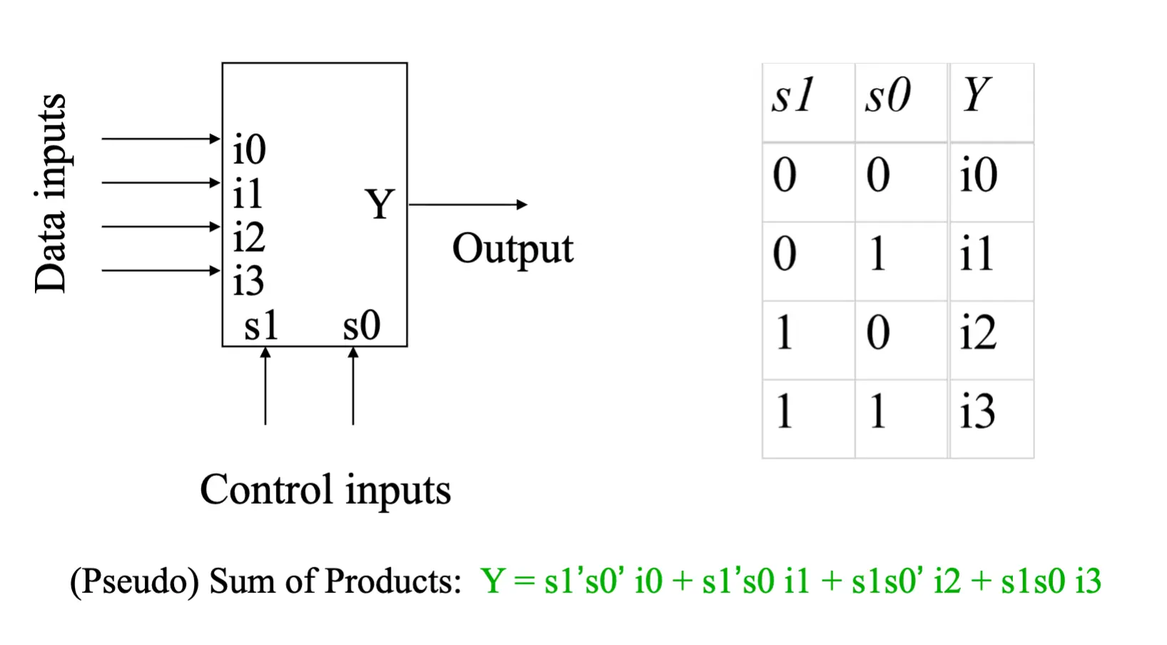
MUX Details
- The diagram above is a truth table for a 2-to-1 MUX
- Can be simplified using boolean algebra
- Implementation: combine AND, OR, NOT gates to match the truth table expression
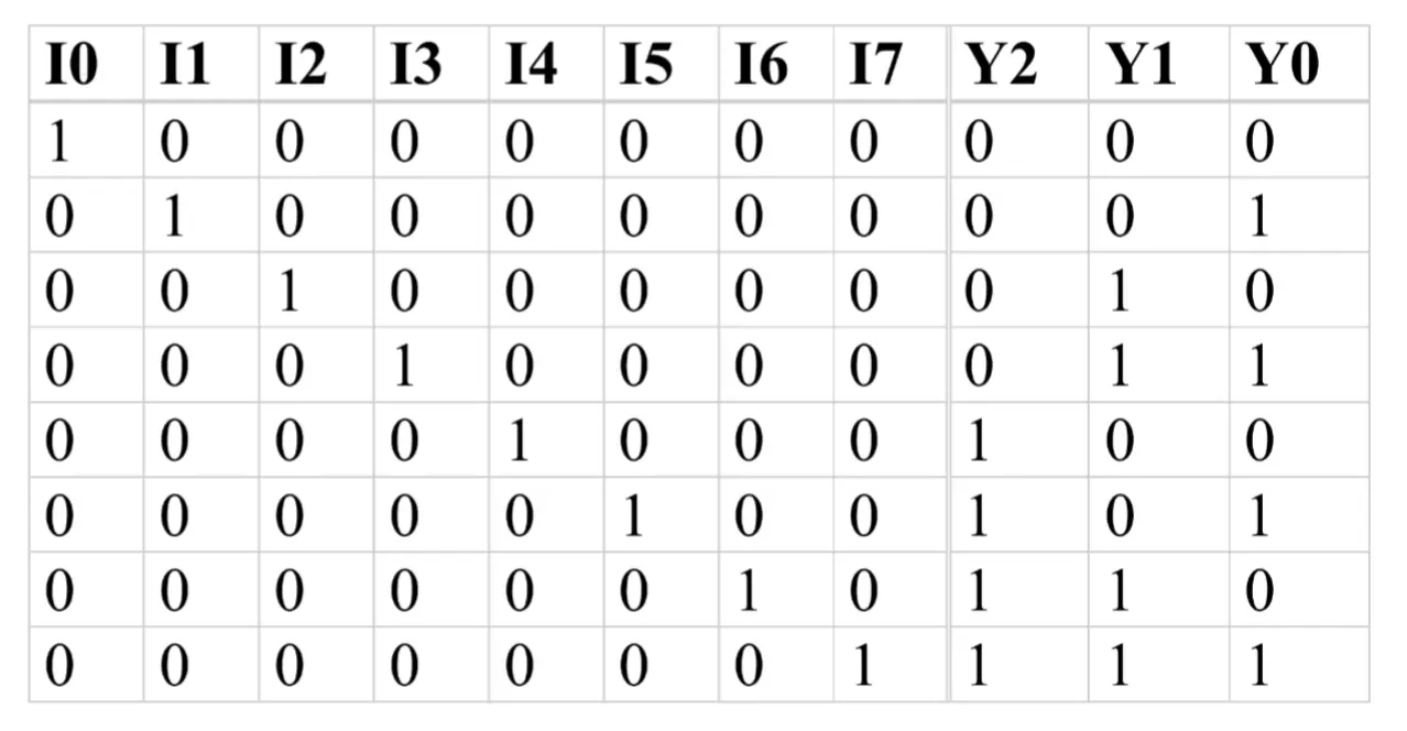
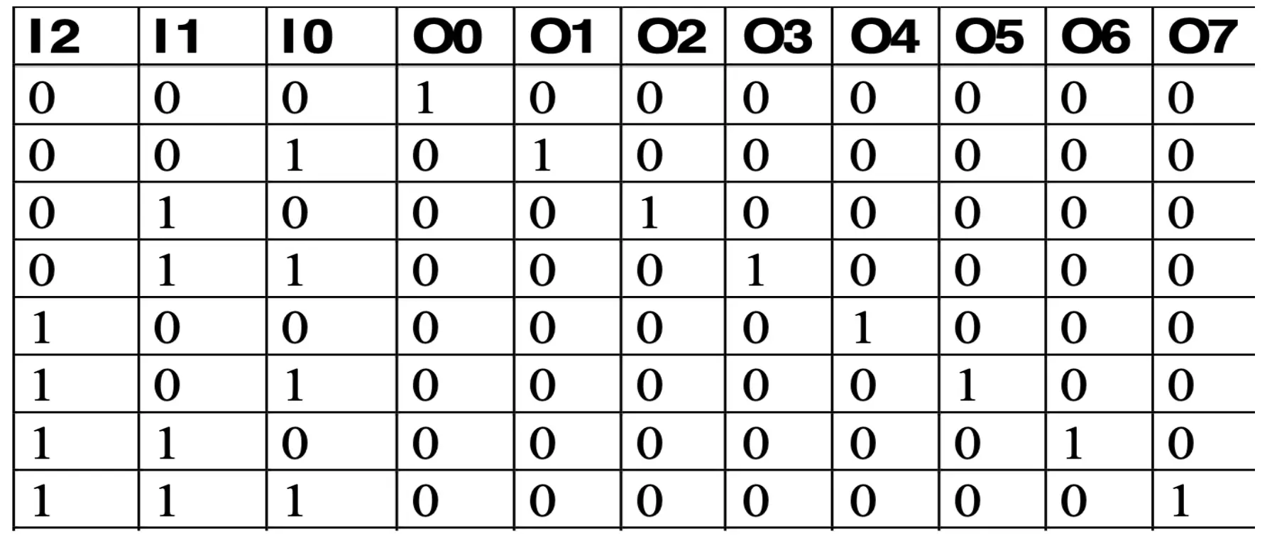
Encoders
- 2ⁿ inputs and n outputs
- Function table for an 8-input encoder → 8 inputs and 3 outputs
Discussion 3: Loops
Translation of If Statements
- C code:
if (condition) {
    <<statements>>
}- Translated to:
    test for negated condition
    bXX EndOfIf       # if negated condition true → skip body
    <<statements>>
EndOfIf:
- Negated condition being true ≡ original condition being false → skip the body
Translation of While Loops
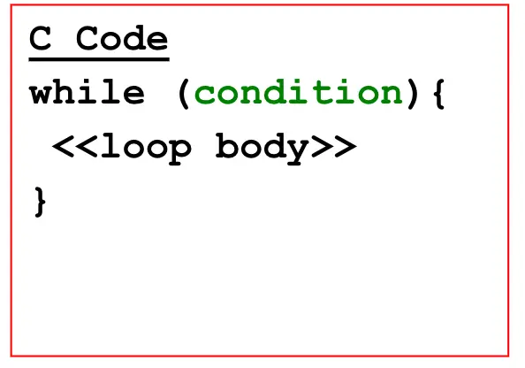
- C code:
while (condition) {
    <<loop body>>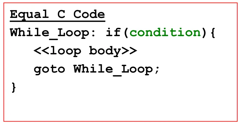
}- Template:
BeginningOfWhile:
    test for negated condition
    bXX EndOfWhile
    <<loop body>>
    j BeginningOfWhile
EndOfWhile:
Example: While Loop Translation
- C code:
i = 0;
sum = 0;
while (i < n) {
    sum += i;
    i++;
}- MIPS assembly (
$t0 = i,$t1 = sum,$t2 = n):
BeginningOfWhile:
    bge  $t0, $t2, EndOfWhile   # if i >= n, exit loop
    add  $t1, $t1, $t0          # sum += i
    addi $t0, $t0, 1            # i++
    j    BeginningOfWhile
EndOfWhile:
For Loops in C
- General form:
for (<<init>>; <<condition>>; <<update>>) {
    <<loop body>>
}- Equivalent while-loop form:
<<init>>
while (<<condition>>) {
    <<loop body>>
    <<update>>
}
Translation of For Loops
- Rewrite as while loop first, then apply while-loop template
- Pattern:
<<init>>
BeginningOfWhile:
    test for negated condition
    bXX EndOfWhile
    <<loop body>>
    <<update>>
    j BeginningOfWhile
EndOfWhile:
Example: For Loop Translation
- C code:
sum = 0;
for (i = 0; i < n; i++) {
    sum += i;
}- MIPS assembly (
$t0 = sum,$t1 = n,$t2 = i):
li   $t0, 0            # sum = 0
# assume $t1 = n
li   $t2, 0            # i = 0
BeginningOfWhile:
    bge  $t2, $t1, EndOfWhile
    add  $t0, $t0, $t2     # sum += i
    addi $t2, $t2, 1       # i++
    j    BeginningOfWhile
EndOfWhile:
Lecture 5: Composite Logic Elements & ALU
Announcements
- Midterm Thursday April 30th, IN CLASS
Midterm Topics
- ISA
- Assembly
- Binary numbers and arithmetic
- Boolean functions
- Gate-level design (mux, decoder, half-adder, full-adder, etc.)
- Transistor implementation of a gate
- One’s and two’s complement and arithmetic
- Anything covered in class, lab, or discussion by April 23rd inclusive
- (Read the book), look at lecture slides, lab/discussion notes
- Difference with the book is the transistor design used
- Any material on the above topics covered in assignments OR class slides OR lab OR discussions can be on the test
- One page, double-sided of notes IS allowed
- NO calculators, NO books
Outline
- More composite logic elements → decoder, comparator, shifter
- 2’s complement arithmetic (covered in discussion)
- Adders → half adder, full adder
- ALU
- Reading: Sec. 3.2.2–3.2.3 and Fig. 4-2 for ALU functional description (except Programmed Logic Arrays)
Where We Are
- So far → gate-level design for boolean functions, plus some composite gates
- Now → more composite gates + how to assemble an ALU
Decoders
- n inputs and 2ⁿ outputs
- Function table for an 8-bit decoder → 3 inputs and 8 outputs
- Exactly one output line is high, determined by the binary value of the inputs
Comparator
- Boolean function, 2 inputs, 1 output
- Out = 1 when two inputs are equal, 0 otherwise
- XOR gate behavior:
- Out = 0 if inputs are both 0 or both 1
- Out = 1 if one input is 1 and the other is 0
- 1-bit comparator →
NOT(XOR(A, B)) - 2-bit comparator →
NOT(OR(XOR(A1, B1), XOR(A0, B0)))- Only 1 when every bit pair matches
Shifters
- Shift-by-one circuits → n-bit input shifted by one bit to the left or right depending on a 1-bit control input
- Example: figure 3-17, page 96
- Implemented with other gates:
- Use AND to “disable” an input → requires a control input
- Use OR to combine the different possibilities (shift left vs shift right vs no shift)
Signed Arithmetic (details in discussion)
- So far only dealt with unsigned numbers → positive by default
- Need a representation for negative numbers:
- Sign-magnitude → devote one bit to sign
- One’s complement
- Two’s complement
- Only 2’s complement is used for integer arithmetic
- Others used in floating-point representation
- Subtraction = addition of 2’s complement of subtrahend
- Bit n−1 is the sign bit → number is positive if this bit is 0, negative otherwise
Half Adder
- Circuit with 2 binary inputs and 2 outputs → generates sum and carry out
- Called “half” because there is no carry input
- Truth table:
| A | B | Sum | Carry |
|---|---|---|---|
| 0 | 0 | 0 | 0 |
| 0 | 1 | 1 | 0 |
| 1 | 0 | 1 | 0 |
| 1 | 1 | 0 | 1 |
- Boolean equations:
- Sum = A XOR B
- Carry = A AND B
Full Adder
- Full adder has an additional carry input (Cin) → 3 inputs (A, B, Cin), 2 outputs (Sum, Carry)
- Sum minterms →
Sum = A'B'Cin + A'BCin' + AB'Cin' + ABCin = Σ(M1, M2, M4, M7) - Carry minterms →
Carry = A'BCin + AB'Cin + ABCin' + ABCin = Σ(M3, M5, M6, M7)
    A  B  Cin | Sum Carry   Min
    ----------|-----------  ---
    0  0  0   |  0   0       0
    0  0  1   |  1   0       1
    0  1  0   |  1   0       2
    0  1  1   |  0   1       3
    1  0  0   |  1   0       4
    1  0  1   |  0   1       5
    1  1  0   |  0   1       6
    1  1  1   |  1   1       7
Arithmetic Circuit Summary
- Half adder → 2-bit input, 2-bit output
- Full adder → 3-bit input, 2-bit output
Ripple Carry Adder
- How to add multi-bit numbers → chain full adders together
- Carry out of bit i feeds into carry in of bit i+1 → carry “ripples” through
     An-1    Bn-1         A1   B1       A0    B0
      |       |            |    |        |    |
      v       v            v    v        v    v
   +-------+            +-------+      +-------+
   |  FA   |  <- ... <- |  FA   | <--  |  FA   | <- Cin (usually 0)
   +-------+            +-------+      +-------+
    |   |                |    |         |    |
    v   v                v    v         v    v
   Cout Sn-1             C1   S1        C0   S0
Subtraction
- How to implement subtraction → add the 2’s complement of the subtrahend
- Steps:
- Invert bits of subtrahend (1’s complement)
- Add 1 using the least-significant carry-in → free, since LSB has an unused Cin input
- How to detect overflow → watch carry in and out of the MSB (Most Significant Bit)
- Also an LSB (Least Significant Bit)
- Details covered in discussion
Hardware Peculiarities — Why We Need a Mux
- Consider:
if (A == B)
    C = D & E;
else
C = D | F;- Software executes either AND or OR, not both
- Hardware is always active → both AND and OR generate outputs whether we need them or not
- Solution → select the desired output
- Outputs not selected are forced to 0 via control signals
- Selected output passes through (
1 · OUT) - All outputs are OR’d together → but only one is actually “passed through”
- Control input is typically generated by the control unit
- This 3-gate (4 counting the NOT) select structure is a multiplexor!
ALU (Arithmetic Logic Unit)
- A functional unit that performs:
- Arithmetic operations → ADD, SUB, MPY
- Logical operations → AND, OR, XOR, NOT
- Operates on data types → 8-, 16-, 32-, or 64-bit values
- Inputs: A (n bits), B (n bits), Cin, M (mode select), S1 S0 (operation select)
- Outputs: F (n bits), Cout
           A[n-1..0]    B[n-1..0]
              |            |
              v            v
          +----------------------+
   Cin -->|         ALU          |--> Cout
          +----------------------+
              |        ^   ^  ^
              v        |   |  |
           F[n-1..0]   M   S1 S0
                       (mode) (op select)
ALU Bit Slice
- Build the ALU from n identical bit slices, each handling one bit position
- Slice i inputs → Ai, Bi, Ci (carry in), M, S1, S0
- Slice i outputs → Fi, Ci+1 (carry out to next slice)
       Ai  Bi   M S1 S0
        |   |    | | |
        v   v    v v v
     +----------------+
Ci ->|    Slice i     |-> Ci+1
     +----------------+
            |
            v
            Fi
ALU Design → Logic Unit + Arithmetic Unit + Mux
- Each bit slice contains:
- Logic unit → computes logical operations on Ai, Bi
- Arithmetic unit → computes arithmetic operations on Ai, Bi, Ci
- Mux (controlled by M) → picks logic or arithmetic result for Fi
Logic Unit
- Controlled by S1, S0 → selects one of 4 logical operations:
| S1 | S0 | Fi |
|---|---|---|
| 0 | 0 | Ai |
| 0 | 1 | NOT(Ai) |
| 1 | 0 | Ai XOR Bi |
| 1 | 1 | Ai XNOR Bi |
Arithmetic Unit
- Built around a full adder with preprocessed inputs X and Y based on S1, S0:
| S1 | S0 | X | Y |
|---|---|---|---|
| 0 | 0 | A | 0 |
| 0 | 1 | A’ | 0 |
| 1 | 0 | A | B |
| 1 | 1 | A’ | B |
- Implementation tricks:
- X = S0 XOR A → flipping A when S0 = 1 gives A’ (one’s complement)
- Y = S1 · B → masks B with S1
- Combined with a Cin of 1 when inverting → gives 2’s complement, enabling subtraction
Packaging Gates
- Many ways to package gates into integrated circuits (ICs)
- Different scales of integration:
- SSI (Small-Scale Integrated) → e.g., TI SN74 series → 4 gates per IC
- MSI (Medium-Scale Integrated)
- LSI (Large-Scale Integrated)
- VLSI (Very Large-Scale Integrated) → e.g., Pentium 4 with several million “gates”
- Different package types → DIP, SSOP, quad flatpack, etc.
SSI: Small-Scale Integration (DIPs)
- DIP = Dual Inline Package
- 14 to 64 pins per package
- Typical contents → 6 INV, or 4 2-input gates, or 3 3-input gates, or 2 complex gates
- Example: 7400 → 3/4 in × 1/3 in, 14 pins
          +---U---+
       1 -|       |- 14  VCC
       2 -|       |- 13
       3 -|  7400 |- 12
       4 -|       |- 11
       5 -|       |- 10
       6 -|       |-  9
  GND  7 -|       |-  8
          +-------+
Discussion 4: ASCII & Memory Access
Representation
- Data in a computer is just binary (0s and 1s)
- Same 32-bit pattern
1111…11111110can mean different things:- Decimal (signed):
-2 - Hex:
0xFFFFFFFE - As four bytes: four separate characters
- Decimal (signed):
- Characters/strings → ASCII → 1 byte per character
ASCII (American Standard Code for Information Interchange)
- Each text character has a unique 8-bit value
- Examples:
S = 0x53,a = 0x61,A = 0x41 - Lower-case and upper-case differ by
0x20(32)A → a: +32a → A: −32
- Other encodings exist (UTF-8, Unicode) but ICS 51 sticks with ASCII
Strings
- Strings = arrays of characters in consecutive bytes of memory
- Variable length → need a way to mark the end
- Convention: NULL-terminated with
'\0'(0x00) "Hello!"→0x48 65 6C 6C 6F 21 00→ 7 bytes, not 6 (the\0counts)
CPU ↔ Memory Interaction
- Initially everything lives in memory: object code (text) + program data
- Registers are much faster storage but there are only 32 of them
- CPU sends address → memory returns data/instruction
   CPU                            Memory
 ┌──────┐    addresses ───→     ┌─────────┐
 │ ALU  │    ←─── data ───→     │ Object  │
 │ Regs │    ←── instr  ───     │  code + │
 └──────┘                        │  data   │
                                 └─────────┘
What’s in Memory
- Text → instructions
- Data
- Global/static → allocated before program begins
- Dynamic → allocated at runtime (heap, stack)
- Memory size: at most 2³² = 4 GB → addresses
0x00000000to0xFFFFFFFF
Memory is Byte-Addressable
- From the programmer’s POV memory is a giant array of bytes (8-bit elements)
- Each byte has its own address: 0, 1, 2, 3, …
- This is true for both MIPS and x86
MIPS Memory Map
0xFFFFFFFC ┌──────────────┐
           │   Reserved   │
0x80000000 ├──────────────┤
0x7FFFFFFC │   Stack      │ ← $sp, $fp  (grows down)
           │      ↓       │
           │ Dynamic Data │
           │      ↑       │
0x10010000 │   Heap       │ ← $gp
0x1000FFFC ├──────────────┤
           │  Static Data │
0x10000000 ├──────────────┤
0x0FFFFFFC │     Text     │ ← $pc, $ra
0x00400000 ├──────────────┤
0x003FFFFC │   Reserved   │
0x00000000 └──────────────┘
- C example mapping:
int f, g, y; int k[10];(globals) → Static Dataint x[10];(local), return addr → Stackmalloc(...)→ Heap (Dynamic)li $t0, 2,add $v0, $t2, $t3(code) → Text
Arrays (HLL)
- Same-type objects stored contiguously under one name
- Syntax in C:
Type Name[Size]int A[10]→ 4 bytes/int × 10 = 40 byteschar B[20]→ 1 byte/char × 20 = 20 bytes
- Can even be an array of arrays (e.g.
char* sports[5]→ array of strings)
Declaring Globals/Arrays in MIPS Assembly
- Goes in the
.datasegment only - Format:
label: data_type comma-separated-list - Common data types:
.asciiz→ null-terminated ASCII string.word→ 32-bit integers.byte→ 8-bit chars or short ints.space N→ reserve N bytes (uninitialized)
- Memory is word-aligned → 32-bit words must start at addresses divisible by 4
- Faster/simpler for the processor
- Mostly transparent to HLL/compiler
1D Array Layout Examples
char foo[5] = {'1','2','3','4','5'};→ MIPS:foo: .byte '1','2','3','4','5'→ 5 byteschar foo[5] = {1,2,3,4,5};→ MIPS:foo: .byte 1,2,3,4,5→ still 5 bytes, but stores raw values 1..5 (NOT ASCII codes for ‘1’..‘5’)int foo[5] = {16, 2, 77, 40, 12071};→ MIPS:foo: .word 16,2,77,40,12071→ 4 bytes × 5 = 20 bytes
Lab 1 Data Section (preview)
- Mixes all three flavors:
.asciiz→ strings (new_line,space,triple_range_lbl, …).word→ arrays of ints (triple_range_test_data,swap_bits_test_data, …).byte→ arrays of chars (hex_digits: .byte '0','1',…,'F')
- In MARS, the data segment view can toggle between ASCII and hex display
Pointers in C → MIPS Equivalents
- C
&(get address) → MIPSla(load address)ptr = &x;↔la $reg, var_name- e.g.
la $t0, hex_digits
- C
*(dereference, get value) → MIPSlw/lb/lbu(read) andsw/sb(write)int x = *ptr;↔lw $dst, imm($reg)*ptr = 5;↔sw $src, imm($reg)$regholds the address;imm($reg)= address + offset
Loading From Memory
lw $dst, imm($reg)→ load a 32-bit wordlb $dst, imm($reg)→ load a byte, sign-extend into the upper bits (use for 2’s complement)lbu $dst, imm($reg)→ load a byte, zero-extend into the upper bits (use for unsigned, e.g. pixels 0–255)
Writing to Memory
sw $src, imm($reg)→ store a word from the full registersb $src, imm($reg)→ store the least significant byte of$src
Example: lb vs lw
hex_digits: .byte 'a','b','c','d'    # 0x61, 0x62, 0x63, 0x64

la $t0, hex_digits
lb $t1, 1($t0)   # → $t1 = 0x00000062     ('b')
lw $t2, 0($t0)   # → $t2 = 0x64636261     (little-endian: 'd''c''b''a')
Size Directives + Endian-ness
- Setup:
my_int: .word 0xDDCCBBAA,la $t0, my_int(assume$t0 = 500) - Little-endian layout (MARS default → x86-style):
addr:   500   501   502   503
byte:   0xAA  0xBB  0xCC  0xDD     ← LSB at lowest address
| Instruction | Result | Why |
|---|---|---|
lb $t1, 0($t0) | 0xFFFFFFAA | byte 0xAA, sign-extended (negative) |
lbu $t1, 0($t0) | 0x000000AA | byte 0xAA, zero-extended |
lw $t1, 0($t0) | 0xDDCCBBAA | full word reassembled |
- For
lw, the address must be word-aligned (multiple of 4) — else error
lb vs lbu — Why It Matters
- Same byte
0xAAinterpreted differently:lb→0xFFFFFFAA→ −86 (signed)lbu→0x000000AA→ 170 (unsigned, e.g. pixel value 0–255)
- Matching instruction families:
- Signed:
add,addi,bge(expansion usesslt) - Unsigned:
addu,addiu,sltu
- Signed:
Endian-ness
- Specifies how multi-byte data is laid out in byte-addressable memory
- Little-endian → LSB at the lowest address (x86, MARS)
- Big-endian → LSB at the highest address
- Same
0xDDCCBBAAstored at address 500:
              Big-Endian      Little-Endian
   500          0xDD              0xAA
   501          0xCC              0xBB
   502          0xBB              0xCC
   503          0xAA              0xDD
lw $t1, 0($t0)→0xDDCCBBAAeither way (the load reassembles correctly)- But
lb $t1, 0($t0)→ reads the byte AT address 500 →0xFFFFFFDD(BE) vs0xFFFFFFAA(LE) - MIPS can be configured either way; MARS uses little-endian, QtSpim follows the host
Loading Array Elements
int array[8] = {1, 2, 3, 4, 5, 6, 7, 8};→ each int = 4 bytes- To load
array[2]:
la $t0, array
lw $t1, 8($t0)        # offset = 2 · 4 = 8 bytes ✓

# WRONG: lw $t1, 2($t0)   → not word-aligned, error
# WRONG: lb $t1, 2($t0) → loads ONE byte from the middle of array[0]- Alternative form (computed address):
la   $t0, array
li   $t2, 8
add  $t3, $t0, $t2
lw   $t1, 0($t3)
Loading Many Elements — Hard-coded vs Loop
int array[32] = {1, 2, …, 32};- Hard-coded → don’t do this:
la $t0, array
lw $t1, 0($t0)
lw $t1, 4($t0)
lw $t1, 8($t0)
...
lw $t1, 124($t0)- Loop → scalable:
la   $t0, array
li   $t2, 32          # counter
my_loop:
    lw   $t1, 0($t0)
    addi $t0, $t0, 4
    addi $t2, $t2, -1
    bne  $t2, $zero, my_loop
Demo 1: ASCII — Same Byte, Different Syscalls (4_ascii_demo.asm)
- A char in MIPS is just a byte → how it prints depends on the syscall code
'a'= 0x61 = 97 → same bits, four different views
.data

.text
.globl main

# utility
print_nl:
    li $a0, '\n'
    li $v0, 11
    syscall
    jr $ra

# main
main:
    li $s0, 'a'

    li $v0, 11        # print_char → 'a'
    move $a0, $s0
    syscall
    jal print_nl

    li $v0, 1         # print_int → 97
    move $a0, $s0
    syscall
    jal print_nl

    li $v0, 34        # print_hex → 0x00000061
    move $a0, $s0
    syscall
    jal print_nl

    li $v0, 35        # print_bin → 0...01100001
    move $a0, $s0
    syscall

    li $v0, 10
syscall- Syscall codes seen here:
11→ print character1→ print integer34→ print hex35→ print binary4→ print string10→ exit
Demo 2: Data Section & Memory Layout (4_data_demo.asm)
.datadeclares labeled storage;.textis where code liveslaloads the address of a label, thenlw/lbread from it with byte offsets- Offsets are in bytes, not elements →
lw $a0, 8($s3)reads the 3rd word (index 2)
.data

my_int:    .word 0xDDCCBBAA

hello_str: .asciiz "Hello!"
bye_str:   .asciiz "Bye..."

int_var:   .word 67305985

int_arr:   .word 1, 2, 3, 4
int8_arr:  .byte 1, 2, 3, 4
char_arr:  .byte '1', '2', '3', '4'

res_10byte: .space 10

dummy_arr: .byte 1, 2, 3, 4

.text
.globl main

# utility
print_nl:
    li $a0, '\n'
    li $v0, 11
    syscall
    jr $ra

# main
main:

    la $t0, my_int
    lw $t1, 1($t0)       # unaligned load — reads bytes at offset 1..4

    la $s0, hello_str
    lb $a0, 5($s0)       # byte at offset 5 → '!'
    li $v0, 11
    syscall
    jal print_nl

    move $a0, $s0        # print whole string → "Hello!"
    li $v0, 4
    syscall
    jal print_nl

    la $s1, char_arr
    lb $a0, 1($s1)       # byte at offset 1 → '2'
    li $v0, 11
    syscall
    jal print_nl

    la $s3, int_arr
    lw $a0, 8($s3)       # word at offset 8 → int_arr[2] = 3
    li $v0, 1
    syscall

    li $a0, '\n'
    li $v0, 11
    syscall

    la $s3, int_arr
    lw $a0, 4($s3)       # word at offset 4 → int_arr[1] = 2
    li $v0, 1
    syscall

    # end program
    li $v0, 10
    syscall
Summary
- ASCII chars are 8-bit (1 byte) values → e.g.
'a' = 0x61 - MIPS Memory Map → text, static data, dynamic data, reserved
- Declare static/global data in
.data(.word,.byte,.asciiz,.space N) - Get an address into a register →
la $reg, var_name - Read/write memory using
$regas a base + byte offset:- Load:
lw,lb(signed),lbu(unsigned) - Store:
sw,sb
- Load:
- Indexing rule: offset =
index · element_size(4 for.word, 1 for.byte) - Word loads/stores require word-aligned addresses (multiples of 4)
- MARS = little-endian → LSB at lowest address
- Same bits, different meanings — interpretation is decided by the instruction width and signed/unsigned variant, not the data itself
Discussion 5: Function Calls, Register Convention & the Stack
Terminology
- Caller → the calling function (e.g.
main) - Callee → the called function (e.g.
sum)
void main() {
  int y;
  y = sum(42, 7);
  ...
}
int sum(int a, int b) {
  return (a + b);
}
Function Conventions (the contract)
- Caller:
- passes arguments to the callee
- “jumps” to the callee
- Callee:
- performs the function
- returns the result to the caller
- returns to the point of call
- must not overwrite registers/memory the caller still needs
Calling with Jumps
- Unconditional jump →
j, orjal+jr j label→ jump to the first instruction afterlabel→PC ← 26-bit address of labeljal label→ jump and link- jumps (same as
j) - stores the address of the instruction after the
jalinto$ra→$ra ← PC + 4
- jumps (same as
jr $reg→ jumps to the address held in$reg→PC ← $reg(e.g.jr $ra)
MIPS Function Conventions
- Call a function →
jal(jump and link) - Return from a function →
jr $ra(jump register) - Arguments →
$a0–$a3 - Return value →
$v0
MIPS Register Set
| Name | Reg # | Usage |
|---|---|---|
$0 | 0 | the constant value 0 |
$at | 1 | assembler temporary (reserved) |
$v0–$v1 | 2–3 | function return values |
$a0–$a3 | 4–7 | function arguments |
$t0–$t7 | 8–15 | temporaries (not preserved across calls) |
$s0–$s7 | 16–23 | saved variables (preserved across calls) |
$t8–$t9 | 24–25 | more temporaries |
$k0–$k1 | 26–27 | OS temporaries (reserved for OS) |
$gp | 28 | global pointer |
$sp | 29 | stack pointer |
$fp | 30 | frame pointer |
$ra | 31 | function return address |
How jal / jr Work Together
0x00400200 main:   jal simple        # jumps to simple; $ra = PC + 4 = 0x00400204
0x00400204         add $s0, $s1, $s2
...
0x00401020 simple: jr $ra # jumps to address in $ra (0x00400204)void→simpledoesn’t return a valuejal→ jumps tosimple, sets$ra = 0x00400204jr $ra→ jumps back to0x00400204(the instruction right after the call)
Passing Arguments & Return Value — diffofsums(2, 3, 4, 5)
int main() {
  int y;
  y = diffofsums(2, 3, 4, 5);   // 4 arguments
}
int diffofsums(int f, int g, int h, int i) {
  int result;
  result = (f + g) - (h + i);
  return result;                // return value
}
# $s0 = y
main:
addi $a0, $0, 2 # argument 0 = 2
addi $a1, $0, 3 # argument 1 = 3
addi $a2, $0, 4 # argument 2 = 4
addi $a3, $0, 5 # argument 3 = 5
jal diffofsums # call function
add $s0, $v0, $0 # y = returned value
# $s0 = result
diffofsums:
add $t0, $a0, $a1 # $t0 = f + g
add $t1, $a2, $a3 # $t1 = h + i
sub $s0, $t0, $t1 # result = (f + g) - (h + i)
add $v0, $s0, $0 # put return value in $v0
jr $ra # return to callerThe Problem: Clobbered Registers
diffofsumsoverwrites 3 registers →$t0,$t1,$s0$s0is supposed to be preserved across calls → ifmainuses$s0to control program flow, the program executes incorrectly- Why not worry about the
$tXregisters? → by convention they’re not preserved, so the caller already knows not to rely on them - Fix →
diffofsumscan use the stack to temporarily store and restore registers
Register Convention (partial)
$t0–$t9→ temporaries → values can change when a subprogram is called (not preserved)$s0–$s8→ saved values → preserved across subprogram calls
Register Convention (full)
| Preserved (Callee-Saved) | Nonpreserved (Caller-Saved) |
|---|---|
$s0–$s7 | $t0–$t9 |
$ra (caller-saved) | $a0–$a3 |
$sp | $v0–$v1 |
stack above $sp | stack below $sp |
Prologue / Epilogue Pattern
- If the callee needs a preserved (
$sX) register, it must wrap the body:- Prologue → push (store) the old value onto the stack
- Epilogue → pop (restore) the old value before returning
- This keeps the caller’s
$s0“good” across the call (the callee failed to follow register convention otherwise)
The Stack
- Memory used to temporarily save variables
- Like a stack of dishes → last-in-first-out (LIFO)
- Expands → uses more memory when more space is needed
- Contracts → frees memory when the space is no longer needed
- Grows down → from higher to lower memory addresses
$sp(stack pointer) → points to the top of the stack
MIPS Memory Map
Address        Segment
0xFFFFFFFC  ┌──────────────┐
            │   Reserved   │
0x80000000  ├──────────────┤
0x7FFFFFFC  │  Stack   ↓   │ ← $sp   (stack grows down)
            │ Dynamic Data │
            │  Heap    ↑   │
0x10010000  ├──────────────┤
0x1000FFFC  │ Static Data  │
0x10000000  ├──────────────┤
0x0FFFFFFC  │     Text     │  (instructions)
0x00400000  ├──────────────┤
0x003FFFFC  │   Reserved   │
0x00000000  └──────────────┘

push → $sp moves down (allocate)    pop → $sp moves up (free)
Storing Saved Registers on the Stack (callee-saved)
# $s0 = result
diffofsums:
  addi $sp, $sp, -4    # Prologue: make space for 1 register
  sw   $s0, 0($sp)     #   store $s0 on stack
                       #   (no need to store $t0 or $t1)
  add  $t0, $a0, $a1   # $t0 = f + g            ┐
  add  $t1, $a2, $a3   # $t1 = h + i            │ Body
  sub  $s0, $t0, $t1   # result = (f+g) - (h+i) │
  add  $v0, $s0, $0    # return value in $v0    ┘
  lw   $s0, 0($sp)     # Epilogue: restore $s0 from stack
  addi $sp, $sp, 4     #   deallocate stack space
  jr   $ra             # return to caller
The Stack During the diffofsums Call
Address Data         Address Data         Address Data
  FC     ?  ← $sp       FC     ?             FC     ?   ← $sp
  F8                    F8    $s0 ← $sp      F8
  F4                    F4                   F4
  F0                    F0                   F0
  (a) Initial State     (b) push($s0)        (c) pop()
- push → store
$s0at F8,$spmoves down to F8 - pop → restore
$s0,$spmoves back up to FC
Nested Function Calls — the $ra Problem
main→simple→easy
0x00400020 main:   jal simple        # $ra = PC + 4 = 0x00400024
0x00400024         add $s0, $s1, $s2
...
0x00400120 simple: jal easy          # $ra = PC + 4 = 0x00400124  ← OVERWRITES old $ra!
0x00400124         jr  $ra
...
0x00400220 easy: jr $ra- Problem → the inner
jal easyoverwrites$ra(0x00400024→0x00400124) - When
simplerunsjr $rait jumps to0x00400124(back insidesimple) instead of returning tomain→ Oops… where is0x00400024? $raonly holds one return address → nesting clobbers it
Fix → Save $ra on the Stack
proc1:
  addi $sp, $sp, -4    # make space on stack
  sw   $ra, 0($sp)     # save $ra on stack
  jal  proc2
  ...
  lw   $ra, 0($sp)     # restore $ra from stack
  addi $sp, $sp, 4     # deallocate stack space
  jr   $ra             # return to caller
Recursive Function Calls
int factorial(int n) {          // 3! = 3·2·1 = 6
  if (n <= 1) return 1;
  else return (n * factorial(n-1));
}factorial(3)→ 3 ·factorial(2)→ 2 ·factorial(1)→ return 1- Each call needs its own
n(and$ra) preserved across the recursive call → use$sXregisters + the stack ($tXwould be clobbered by the recursive call)
0x90 factorial: addi $sp, $sp, -8    # Prologue: make space (2 words)
0x94            sw   $ra, 0($sp)     #   store $ra
0x98            sw   $s0, 4($sp)     #   store $s0
0x9C            addi $t0, $0, 2
0xA0            slt  $t0, $a0, $t0   # n < 2 ?  (i.e. n <= 1)
0xA4            beq  $t0, $0, else   # no  → go to else
0xA8            addi $v0, $0, 1      # yes → return 1
0xAC            j    end             #       jump to epilogue
0xB0 else:      move $s0, $a0        # save n into $s0
0xB4            addi $a0, $s0, -1    # n = n - 1
0xB8            jal  factorial       # recursive call
0xBC            mul  $v0, $s0, $v0   # n · factorial(n-1)
0xC0 end:       lw   $ra, 0($sp)     # Epilogue: restore $ra
0xC4            lw   $s0, 4($sp)     #   restore $s0
0xC8            addi $sp, $sp, 8     #   release space
0xCC            jr   $ra             # return
Stack During the Recursive Call (3! = 6)
Each frame = 2 words: [ $ra @ low addr, $s0 @ high addr ]

      Deepest recursion              Unwinding (returns)
   Address Data                   Address Data
     FC                  ← $sp       FC            $v0 = 6  (final)
     F8    $s0                       F8    $s0
     F4    $ra                       F4    $ra     ← $sp   $s0=3, $v0 = 3·2 = 6
     F0    $s0 (0x3)                 F0    $s0 (0x3)
     EC    $ra (0xBC)                EC    $ra     ← $sp   $s0=2, $v0 = 2·1 = 2
     E8    $s0 (0x2)                 E8    $s0 (0x2)
     E4    $ra (0xBC)    ← $sp       E4    $ra     ← $sp   $s0=1, $v0 = 1
- Each recursive call pushes its own
$ra+$s0(the currentn) - On the way back, each frame is popped and the multiply runs → 1 → 2·1 → 3·2 = 6
Function Call Summary
- Caller:
- put arguments in
$a0–$a3 - save any needed registers (
$ra, maybe$t0–$t9) jal callee- look for the result in
$v0 - restore registers
- put arguments in
- Callee:
- save registers that might be disturbed (
$s0–$s7) - perform the function
- put the result in
$v0 - restore saved registers
jr $ra
- save registers that might be disturbed (
Discussion 6: System Calls (syscall)
What syscall Is
syscall→ requests a system service from the OS/simulator- Used for:
- Input/output → read from console / file / external device; print to console, write to file / device
- random numbers, time, sleep, …
$v0→ holds the service number (which service you want)- plus other argument values, if any
- Full list → MARS help menu (F1), or the MIPS syscall function reference in MARS
Steps to Use a syscall
- Load the service number into
$v0 - Load argument values (if any) into
$a0,$a1,$a2, or$f12as specified - Issue the
syscallinstruction - Retrieve return values (if any) from the specified result registers
Lab0: Two Services (no global variables)
- Print an integer to the console → service
1
li   $v0, 1
move $a0, $s0
syscall- Exit the program → service
10
li $v0, 10
syscall
Printing Characters & Strings (Lab2 main)
- Print a string → service
4
li $v0, 4
la $a0, change_case_output
syscall- How do you know the end of a string? → the NULL terminator
'\0' - Print the 1st char → service
11(print char)
li $v0, 11
la $t0, change_case_output    # address of the string
lb $a0, 0($t0)                # load the 1st byte (the char value)
syscall- For the 2nd char → use offset
1($t0) - Address vs. value distinction:
la $t0, label→ loads the addresslb $a0, 0($t0)→ loads the value of the char at that address
Common Print Services
| Service | $v0 | Arguments |
|---|---|---|
| print integer | 1 | $a0 = integer |
| print string | 4 | $a0 = address of string |
| print char | 11 | $a0 = char value |
| exit | 10 | — |
Demo: Print globals & arrays (4_data_demo.asm)
- Print a string
- Print a single character from a string
- Print elements from a char array
- Print elements from an int array
File I/O — Must Open First
- Must open a file before reading/writing it
- Concept → like C
FILE *fptr = fopen("myFile.dat", "r");or Pythonf = open("myFile.dat", "r")→ returns a file descriptor - In MIPS assembly → low-level → use
syscallto obtain the file descriptor directly - Read → reads bytes into a buffer (like C
fgets(str, 4, fptr)/ Pythonf.read(4))
File I/O syscall Table
| Service | Code | Arguments | Result |
|---|---|---|---|
| open file | 13 | $a0 = addr of null-terminated filename; $a1 = flags; $a2 = mode | $v0 = file descriptor (negative if error) |
| read from file | 14 | $a0 = file descriptor; $a1 = addr of input buffer; $a2 = max chars to read | $v0 = # chars read (0 if EOF, negative if error) |
| write to file | 15 | $a0 = file descriptor; $a1 = addr of output buffer; $a2 = # chars to write | $v0 = # chars written (negative if error) |
| close file | 16 | $a0 = file descriptor | — |
- Open flags →
0= read,1= write
Example: Open / Write / Close (from F1 Help Menu)
.data
fout:   .asciiz "testout.txt"                         # filename for output
buffer: .asciiz "The quick brown fox jumps over the lazy dog."

.text
# Open (for writing) a file that does not exist
li   $v0, 13          # system call for open file
la   $a0, fout        # output file name
li   $a1, 1           # flags → open for writing (0 = read, 1 = write)
li   $a2, 0           # mode is ignored
syscall
move $s6, $v0         # save the file descriptor

# Write to the file just opened
li   $v0, 15          # system call for write to file
move $a0, $s6         # file descriptor
la   $a1, buffer      # address of buffer to write from
li   $a2, 44          # hardcoded buffer length (# chars)
syscall

# Close the file
li   $v0, 16          # system call for close file
move $a0, $s6         # file descriptor to close
syscall- Be careful with
$sXhere → register convention applies- may replace with
$tX, or use$spto save/restore
- may replace with
- To read a file instead → change the syscall types (open with flag
0, then use service14)
Summary
syscall→ ask the OS/MARS for a service; the service number goes in$v0- Pattern → set
$v0(+$a0/$a1/$a2/$f12args) →syscall→ read result registers - Common codes →
1print int,4print string,11print char,10exit - Files → must open (13) before read (14) / write (15), then close (16);
$v0returns the file descriptor (negative = error)
Lecture 6: Memory — Latches
Today’s Objectives
- Ideal vs real gates
- Sequential circuits
- Latch
- Clock
- Brief look at processor organization
- Reading: Sec. 3.3.1–3.3.4
Storage Elements
- So far → only memoryless digital functions (combinational logic)
- Now we need to store program data and intermediate values → sequential logic
- The ISA tells us there are registers and memory → e.g.
ADD R4, R6:- where does the data reside? What are
R4,R6? How do they work?
- where does the data reside? What are
- Built from gates, similar to combinational logic, BUT:
- require feedback → new state = F(current state, inputs)
- require timing to be taken into account → assume non-zero gate delay → introduce the clock
- A combinational circuit has latency DT → output changes DT seconds after an input change, and keeps changing as long as the inputs change
- New state → a boolean function depending on the inputs from DT earlier + the state from DT earlier
SR Latch (Set-Reset) — a basic storage element
- Two cross-coupled NOR gates → Q and Q’ are fed back as inputs → this is what makes it sequential
- A bi-stable circuit that stores a binary value:
- Q = 1 → “1” state
- Q = 0 → “0” state
- Can only be in one of these states → output change requires S or R to be applied
   R ──▶[ NOR ]──┬──────────▶ Q
           ▲     │
           └──── │ ────┐   (cross-coupled: Q feeds the bottom NOR,
           ┌──── │ ────┘    Q' feeds the top NOR)
           ▼     │
   S ──▶[ NOR ]──┴──────────▶ Q'
- Behavior:
- S = 1, R = 0 → Set → Q = 1
- S = 0, R = 1 → Reset → Q = 0
- S = R = 0 → hold (Q unchanged)
- S = R = 1 → forbidden → unstable; Q may oscillate before settling to 1 or 0
SR Latch Truth Table
| Qt | S | R | Qt+1 |
|---|---|---|---|
| 0 | 0 | 0 | 0 |
| 0 | 0 | 1 | 0 |
| 0 | 1 | 0 | 1 |
| 0 | 1 | 1 | ? |
| 1 | 0 | 0 | 1 |
| 1 | 0 | 1 | 0 |
| 1 | 1 | 0 | 1 |
| 1 | 1 | 1 | ? |
?→ undefined output (the S = R = 1 problem)
Problem with the SR Latch
- Combinational functions take time to settle → the output may vary for a while before reaching the correct value
- If S or R change, Q changes immediately → but we want changes to happen only when desired and once per clock cycle
- Fix → modify the latch to incorporate the clock as an input
The Clock
- We’ll build a computer with many latches → need to make sure things happen when required
- Example arithmetic operation:
- take data from 2 registers → run through the ALU → store to another register
- these three steps must occur at the right time
- Solution → generate and distribute a special signal called the clock
- keeps time → like a conductor for an orchestra or a drummer in a band
- Any state change in the system is referenced to the clock
- The clock is the basic time unit for executing instructions (an instruction may take several clocks)
- Must account for signal propagation through gates → typical gate delay today < 100 ps (10⁻¹⁰ s)
Clocked SR Latch
- We want gate outputs to change only at specific times → add circuitry so changes occur only when the clock is active (Clock = 1)
- Add two gates in front of the NOR latch, gated by the clock:
- if Clock = 0 → neither S nor R reaches the NOR gates → Q holds
- if Clock = 1 → S/R pass through → Q can change
   S ───┬──[ AND ]──┐
        │     │     │
 Clock ─┼─────┤  [ SR latch ]──▶ Q, Q'
        │     │     │
   R ───┴──[ AND ]──┘
- Q only changes when Clock = 1
- Timing → S, R come from elsewhere in the system; they can only take effect after the clock goes high (DT1 later); Q then changes DT2 later, due to gate propagation delay
Still Have Problems
- (A) Undefined state when S = R = 1 → solved by the D latch (next)
- (B) Inputs can change as long as the clock is high → half a clock cycle → that’s too long
- could play with the duty cycle (% of the cycle that is “1”) → generate a very narrow “1” pulse → but hard, especially at 4 GHz
- “sample” the input only while the clock is “1”
- better solution → flip-flops (later)
D Latch — avoiding S = R = 1
- Only one data input: D (plus the clock)
- D drives S directly; D’ (inverted D) drives R → S and R can never both be 1
- When the clock becomes 1:
- D = 1 → the circuit remembers 1 (Q = 1)
- D = 0 → the circuit remembers 0 (Q = 0)
   D ──┬────────────[ AND ]──┐
       │              │       │
       │      Clock ──┤   [ SR latch ]──▶ Q, Q'
       │              │       │
       └──[ NOT ]─────[ AND ]──┘
8-Bit Memory
- Use 8 D latches → an 8-bit memory
- 8 inputs (D0–D7), all written at the same time → all 8 latches share the same clock
        D0 ──[ D Latch ]── Q0
        D1 ──[ D Latch ]── Q1
        D2 ──[ D Latch ]── Q2
         ⋮                  ⋮
        D7 ──[ D Latch ]── Q7
                 ▲
              clock (shared)
Registers
- A register → a group of latches/flip-flops treated as one unit, instead of addressing each storage element individually
   Data_in[7:0] ──▶│  Register A  │──▶ Data_out[7:0]
                        ▲
                      Clock
Lecture 7: Flip-Flops & RAM
Flip-Flops
- D latches still have a problem → input changes while the clock is “1” still propagate
- Another (better) solution to the SR-latch input-change problem
- Two approaches:
- Master-slave flip-flops
- Edge-triggered flip-flops
- Change can occur only on a clock edge (transition 0→1 or 1→0) → exactly one change per clock cycle, output stable for the whole clock period
D Flip-Flop Timing
- D (data) can wander, but Q only updates on the active clock edge → Q is stable between edges
Master-Slave D Flip-Flop
- Two D latches in series:
- Master latch → clocked by Clk
- Slave latch → clocked by Clk’ (the inverted clock)
   D ──▶│ D    Q │── Qm ──▶│ D    Q │──▶ Q
        │ Master │         │ Slave  │
 Clk ─┬▶│ Clk    │     ┌──▶│ Clk Q' │──▶ Q'
      │  └────────┘     │   └────────┘
      └────[ NOT ]──────┘  Clk'
- When Clk is high → the master is transparent → Qm follows D (slave holds, since Clk’ = 0)
- When Clk is low → the slave is transparent → Q follows Qm (master holds)
- The output changes at the clock edge that falls from 1 → 0 → this D FF is negative-edge triggered
Random Access Memory (RAM)
- Access time → from address presented to data out
- Constant access time → independent of the address (unlike tape or disk, which are sequential)
- Semiconductor memory → RAM and ROM
- Many bits on one IC → each bit is a “latch”
- Two types (speed / cost / size tradeoff):
- SRAM (Static) → faster, fewer bits → each bit is a latch
- DRAM (Dynamic) → denser/cheaper → each bit stores charge on a tiny capacitor
- Tradeoff → higher speed costs more per bit and limits capacity
Memory Cell Organization
- SRAM cell → a clocked D-latch-style cell:
   Data_in ──▶│ D       │
   Clock ─────▶│ C    Q │──▶ Data_out
   Write ─────▶│ En      │
- DRAM cell → one transistor controls access to a capacitor that stores charge:
- Write → put charge in
- Read → let charge flow out (destructive → needs refresh)
Register File
- An array of registers (R0…R7) addressed as a unit
- Write path → an address decoder drives the Enable of the selected register → only that register loads
Data_inon the clock - Read path → an address-controlled mux selects the addressed register’s Q →
Data_out - For 8 registers → a 3-bit address
   Data_in ─┬──▶│ D  R0  Q │─┐
            ├──▶│ D  R1  Q │─┤
            │        ⋮       ├─[ MUX ]──▶ Data_out
            └──▶│ D  R7  Q │─┘     ▲
                   ▲               │
   Address ─▶[ decoder ]───────────┘
   (3 bits)   (drives Enable)   (selects output)
                   ▲
                 Clock
Lecture 8: More Memory — Organization & Decoding
Today’s Objectives
- Continue the study of memory organization
- Reading: Sec. 3.3.1–3.3.4, Sec. 2.1 pp. 39–42, Sec. 4.1.1–2 (next time)
Review
- SR latch → basic storage device, but the output changes as the inputs change
- Clock & clocked latches → better control of when the output changes
- Flip-flops → best way to store data, based on the clock’s rising edge → one change per clock cycle, output stable for the whole period
- Registers → aggregate a number of latches/flip-flops, controlled as a unit
- Register file → array of registers (see Lecture 7)
Memory Chips
- A memory IC is typically organized as a cell matrix → NxN (good for layout)
- At each position → a single cell (1 bit)
- To get a wider output → replicate the matrix
- e.g. a 128 Mb IC may have 8 blocks (individual NxN matrices)
- Memory is built out of multiple chips
- e.g. a 256 MB DIMM may have 16 × 128 Mb ICs → eight are read/written at once, delivering 8 bits (a byte)
Memory Organization & Decoding
- A decoder circuit selects the appropriate word in memory based on the address provided
- Two steps:
- first → a row is read out of the cell matrix, N bits at once
- second → a bit (column) is selected from that row and output
- The output goes through a tri-state buffer → 3 states: 0, 1, floating (electrically disconnected)
- The larger the memory → the longer it takes to read
- SRAM is faster than DRAM but has fewer bits:
- SRAM “bit” → a latch
- DRAM “bit” → a special transistor (capacitor + access transistor)
Memory IC Organization (NxN, 1 bit wide)
   Data_in
      │
      ▼
   ┌───────────────────────┐
   │  ▢   ▢   •••   ▢       │ ◀── row selected by Row Address
   │  ▢   ▢          ▢      │
   │         •••            │     (▢ = single cell)
   │  ▢   ▢          ▢      │
   └───┬───┬───────┬────────┘
  Row  │   │       │
  Addr ▼   ▼       ▼
       [  column MUX  ] ◀── Column Address
              │
              ▼
         [ tri-state ] ◀── Output Enable (OE)
              │
              ▼
           Data_out
- Row Address → row decoder selects one row (N bits read at once)
- Column Address → mux selects 1 bit from that row
- OE → enables the tri-state buffer onto the output
RAM Control
- Multiple chips are connected together to → get a wider word, or get a larger memory
- Need to be able to → select a chip and enable its output
- Control signals:
- CS (chip select) → nothing happens inside a RAM unless it is selected
- OE (output enable) → allows direct connection of IC outputs (tri-state onto a shared bus)
- R/W’ → read or write
A 4-Chip Memory System
   Data_Bus ═══════════╦════════════╦════════════╦═══════════
                       │            │            │
               ┌───────┴───┐ ┌──────┴────┐      ┌┴──────────┐
   Addr ──────▶│ Din  Dout │ │ Din  Dout │ •••  │ Din  Dout │
   R/W' ──────▶│ Addr RAM0 │ │ Addr RAM1 │      │ Addr RAM3 │
               │ R/W'    OE│ │ R/W'    OE│      │ R/W'    OE│
               │ CS        │ │ CS        │      │ CS        │
               └────▲──────┘ └────▲──────┘      └────▲──────┘
                    │             │                  │
   Address ─▶[ decoder ]─CS0──────┴─CS1──────────────┴─CS3
   Output_enable ────────(OE, shared)
   R/W' ─────────────────(shared)
- Low address bits →
Addr(shared by all chips) - High address bits → decoder → one CS per chip → selects the active chip
- Only the selected chip (with OE asserted) drives the shared data bus
Lecture 9: Disk Memory, Error Detection/Correction & Compression
Today’s Objectives
- Disk memory
- Error correction & detection
- Full data path organization (next lecture)
- Reading: Sec. 2.3.2 (disk), Sec. 4.1.1 (ignore JVM stuff), class slides
Disk Memory
- Disk → magnetic memory
- “Sequential” access (mechanical positioning)
- Reads/writes are performed on blocks of data → more efficient this way
- Much slower than memory → milliseconds to access, even at 15K RPM
- Much larger than main memory (DRAM) → multiple TB common (and growing)
Disk Structure
- A disk = a stack of platters, each with two recording surfaces
- A mechanical arm moves the read/write head across the surfaces
- Each surface → data on concentric circles called tracks, further divided into sectors (marked by a sector mark)
   ════════ Surface 1     ◀── direction of arm
   ════════ Surface 2
   ════════ Surface 3
   ════════ Surface 4
        ⋮
   (head moves in/out to reach the desired track)

   One platter (top view):  Track 0 (outer) … Track N (inner),
   each divided into sectors
Disk Organization — Terms
- Track → sequence of bits at the same radius on one surface
- Cylinder → set of tracks at the same radius across all platters
- Sector → fixed-length segment within a track
- Seek time → time to position the head over a track
- Rotational latency → time for the disk to rotate the desired sector under the head
- Head transfer rate → how fast data transfers once the head is in position
Parameters
- Rotational speed → 3600 to 15K RPM → determines how soon the data appears under the head
- Seek speed → track-to-track → milliseconds
- Average time to find data → ½ rotational delay + average seek time
- ~100 ns for DRAM vs ~15 ms for disk → orders of magnitude slower
- Transfer rate → ~100 MB/sec
Operation
- Address supplied as (platter, track, sector)
-
- Seek → move the arm + R/W head assembly to the desired track
-
- Locate the sector → wait for the platter to rotate to the right place
-
- Read/write the sector
- Can read more at once → a whole cylinder → read the track from all platters at once
Optimization
- Read an entire sector / track / cylinder → helps amortize the startup cost
- Cache the read data in the controller’s memory → satisfies future requests from RAM (works due to locality)
- The disk controller + OS may reorder disk I/O requests to minimize seek time
Error Detection & Correction
- Data stored in bulk, or transmitted, can be corrupted
- Causes of corruption are diverse; occurrence is relatively infrequent
Error Detection — Parity (simplest method)
- When writing/sending a block → add a parity bit indicating whether the number of 1s is even (or odd)
- When reading/receiving → recompute and check the count
- If the written parity ≠ the read parity → an error was detected
                 P │←──── Data bits ────→
   Transmitted:  0 │ 1 0 0 1 0 1 1     (four 1s → even → P = 0)
                 P │       ↓ error
   Received:     0 │ 0 0 0 1 0 1 1     (three 1s → odd → mismatch ⟹ error!)
- Detects a single-bit error, but cannot say which bit, and cannot fix it
Error Correction — Hamming Codes
- Use multiple parity bits, each checking an overlapping subset of the data bits
- The combined parity bits name the position of the wrong bit → so it can be corrected
Compression — Huffman Coding
- A lossless compression algorithm
- Each symbol is encoded in a bit string whose length is “proportional” to its frequency of occurrence
- frequent symbols (e.g. “e”) → shorter codes; rare symbols (e.g. “x”) → longer codes → saves a lot of bits on real text
- Built by constructing a prefix tree → guarantees no encoding is a prefix of another (so it decodes unambiguously)
- Build bottom-up → repeatedly combine the two lowest-probability nodes
Huffman Example
- Symbols and probabilities:
| Symbol | Probability |
|---|---|
| A | 0.3 |
| B | 0.3 |
| C | 0.2 |
| D | 0.1 |
| E | 0.1 |
- Build (combine the two lowest each step; label branches 1 / 0):
- D(0.1) + E(0.1) → DE(0.2)
- C(0.2) + DE(0.2) → CDE(0.4)
- A(0.3) + B(0.3) → AB(0.6)
- AB(0.6) + CDE(0.4) → root(1.0)
                root
            1 /      \ 0
            AB         CDE
          1/  \0     1/    \0
          A    B     C      DE
                           1/  \0
                           D    E
- Resulting encoding:
| Symbol | Encoding |
|---|---|
| A | 11 |
| B | 10 |
| C | 01 |
| D | 001 |
| E | 000 |
- Example →
AABCBDAE→11 11 10 01 10 001 11 000=111110011000111000→ 18 bits - A fixed 3-bit code → 8 chars × 3 bits = 24 bits → Huffman saves 6 bits here
Lecture 10: Data Path & Control Unit
Back to the CPU — the Final Stretch
- Goal → design the control unit and put it all together
- Reading: Sec. 4.1.1 (ignore JVM stuff), class slides
Data Path
- The core of the CPU → a register file feeding an ALU
- Read two operands from the register file (
Reg_addr A,Reg_addr B) onto buses A and B - The ALU computes a result; flags N, C, Z are produced; the Result bus writes back to the register file
   Result addr ─▶┌───────────────┐◀─ Reg_addr A
                 │ Register File │◀─ Reg_addr B
                 └──┬─────────┬──┘
                    │ A       │ B
                    ▼         ▼
   ALU op ─▶ ┌───────────────────┐ ─▶ Z
   Cin   ─▶  │        ALU        │ ─▶ N
             └─────────┬─────────┘ ─▶ C
                       │ Result
                       └──────────────▶ (back to Register File)
Data Path Operation
- Read operands from the register file → at the current rising clock edge → place on buses A and B
- Specify the ALU operation
- “Wait” for the ALU → designed to fit into 1 clock cycle (no real wait)
- Set flags → N, C, Z
- Write the RESULT bus to the selected register → really happens on the next rising edge
Adding Memory Access
- Memory for our machine → a linear array of words (each word 2/4/8 bytes), byte-addressable even if organized as words
- Two steps → generate a memory address, then access memory at that address
- Read → wait for data ready → read into the Memory Data Register → move to the register file or ALU
- Write → put data out to memory
- Need two new registers → a clocked interface to the asynchronous memory:
- MAR (Memory Address Register)
- MDR (Memory Data Register)
- Control signals → R/W’ and D_ready (data ready on read / “done” on write)
Register Transfer Language (RTL)
- A shorthand for describing register-to-register (and all other) data-path operations, and control logic
- Everything comes from and goes to a register → so it can be described as register transfers through combinational logic
- Notation:
- variables = (contents of) registers
- operations = assignment, arithmetic, logical, etc.
- memory = an array →
M[4](orR[4]) = location 4 of memory (or the register file) - assignment →
R[4] ← R[4] + R[6] - conditional →
Z ← 1 if R[4] = 0 - simultaneous ops (in time) →
MDR ← Mem[MAR] ; PC ← PC + 2
- Example → RTL for
Ld Rj, Ri:MAR ← Ri(orRi + displacement)MDR ← Mem[MAR]ifD_ready = 1Rj ← MDR
Instruction Execution & Fetch
- Instruction execution includes steps beyond the specified operation → the same data path is reused for both data processing and these extra steps → keep augmenting it until it can do everything
- Need logic to execute the control algorithm → a control unit
- Instruction fetch → get an instruction from memory to start → needs two more registers:
- PC (program counter) →
PC ← PC + 2 - IR (instruction register) →
IR ← Mem[PC]
- PC (program counter) →
- Plus the control signals to drive all this
Full (Augmented) Data Path
- Adds the memory-interface registers and the selection muxes around the core register-file / ALU:
            ┌────────┐       EnblRes│      Addr_A│  Addr_B│
            │        │  Addr_Res ▼  ▼            ▼        ▼
            │ Memory │◀────────▶┌───────────────┐
            │        │          │ Register File │
            └───┬────┘          └───┬───────┬───┘    Const
       Sel_mem  │   ┌──[ PC ]       │       │         │
         [MUX]──┴───┤  [ MAR ]    [Sel_A] [Sel_B]◀────┘
                    │  [ MDR ]──┐    │ A     │ B
                    │  [ IR ]   │    ▼       ▼
                    │           │ ┌───────────────┐
                    └───────────┘ │      ALU      │◀── Op
              D_ready             └───────┬───────┘
                                          │ Result
              ──▶ To Control Unit (flags Z / N / C, IR opcode)
- New registers → PC, MAR, MDR, IR
- New muxes →
Sel_mem(address source: PC vs Result),Sel_A(ALU A input: reg file vs PC),Sel_B(ALU B input: reg file vs Const) - Write-enable controls →
Wr_PC,Wr_MAR,Wr_MDR,Wr_IR,EnblRes
Control Unit
- Generates the control signals for the data path
- Encoded as microinstructions (control words, CW) → a format with various fields
- Driven by a microcode engine → supplies one CW per cycle
Control Word (CW) Format
- Groups of control signals → memory, ALU, PC, etc.
| R/W' | Sel_M | Wr_MAR | Wr_MDR | Wr_IR | EnblRes | Sel_A | Sel_B | Op | Wr_PC | ... |
|◀──── Memory Control Group ────▶|◀────────── ALU / Reg Control ─────────▶| PC | Etc.|
Microcode Engine
- Cycle (do forever):
- fetch the m-instruction →
CW ← m-Mem[m-PC] - update m-PC →
m-PC ← CW.Next(a field in the CW; more general thanm-PC ← m-PC + 1) - apply the CW → run a wire from each CW bit out as a control signal
- wait for the end of the cycle
- fetch the m-instruction →
- Very simple → a tiny CPU whose only job is “fetch m-instruction, update m-PC”
- Location N in the m-store → the first CW of the m-code → the first CW of CPU instruction-fetch → on hardware reset,
m-PC ← N - m-PC uses an extra next-address field in the CW itself → simplifies branching and allows easy relocation of m-instructions
- Two “next” addresses:
- Next1 → next sequential address (same as
m-PC + 1, but eliminates an adder) - Next2 → conditional m-branch target
- Next1 → next sequential address (same as
Microcode Engine Organization
        ┌─────────────────┐   Addr     m-PC
        │ m-program store │◀──────────── │
        └────────┬────────┘              ▲
            CW   │ Data              [ MUX ]◀── B_sel
   ┌─────────────▼───────────────────────┐  ▲ ▲ ▲ ▲
   │ Mem | ALU | Reg | Branch | PC | Next1 | Next2 |  Reset_addr   IR.opcode
   └──┬──────────────────┬─────────────────┘    ▲
      │ control          │ Branch field          │
      ▼ signals          ▼                 [ B_sel Generator ]◀── Z, N, D_ready
   (to CPU data path)                       ◀── IR (Opcode, R1, R2)
- The CW’s Next1 (sequential) and Next2 (branch target) feed a mux
- The B_sel Generator picks the next m-PC source using the Branch field + the selected flag
m-Branches
- Reasons to have a microcode branch:
- waiting for memory (
D_ready = 1) - implementing CPU branch instructions (BN, BZ, …)
- instruction decode → branch to the right CW for the fetched opcode
- waiting for memory (
- Conditional m-branch →
if cond then m-PC ← Next2 else m-PC ← Next1 - Unconditional m-branch →
m-PC ← Next1
Branch Field in the CW
- 4 bits → specify which input signal to branch on (one-hot — only one bit may be 1):
1000→ branch on Z0100→ branch on N0010→ branch on Opcode (instruction decode)0001→ branch on D_ready0000→ do not branch
- RTL for the m-branch:
- Z type → if Z = 1 then
m-PC ← Next2elseNext1 - N type → if N = 1 then
m-PC ← Next2elseNext1 - Opcode →
m-PC ← IR.opcode(no arithmetic — just jam the value in) - D_ready → if D_ready = 1 then
m-PC ← Next2elseNext1 0000→m-PC ← Next1
- Z type → if Z = 1 then
- B_sel Generator → selects the next m-PC via a mux, based on the branch type + the value of the selected control signal
Instruction Decode
- Implemented as a microcode branch →
m-PC ← IR[opcode]→ no arithmetic, just jam the value in - At each opcode address → a group of CWs implementing all the steps of that instruction (I-fetch, PC update, I-decode, the RR ALU op, …)
- For a whole instruction group → use further decoding on some opcode bits to pick the actual instruction
Microprograms
- Represented with symbolic notation (equivalent to the m-store contents, minus labels)
- Tools (compilers/assemblers) generate the CW bit strings → nobody would want to do it by hand
- The full m-program implements all CPU instructions
- Convention for writing them → only show the signals that must be “1” for the next clock (the rest are don’t-care)
- use
Iden= pass-through ALU function →Result ← B - register specifiers x, y come from
IR.r1,IR.r2
- use